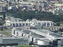
CEA-Leti: Laboratoire d'électronique des technologies de l'information
CEA-Leti is a research institute for electronics and information technologies, based in Grenoble, France. It is one of the world's largest organizations for applied research in microelectronics and nanotechnology.
 | |
| Type | Non-profit research institute |
|---|---|
| Founded | 1967 |
| Headquarters | , |
Key people | Emmanuel Sabonnadière, director |
| Parent | Direction de la Recherche Technologique |
Overview
A subsidiary of the Commissariat à l’Energie Atomique et aux Energies Alternatives (CEA) France's nuclear and renewable energy commission, Leti was established in 1967 in Grenoble, a university town in the French Alps that has now become an internationally recognized scientific hub. Today, the CEA-Leti is granted over 286 patents a year and handles a portfolio of more than 3,100 patented inventions.
The institute employs 1,900 people, while training more than 162 graduate students (38% foreigners), 36 PostDoc and hosting 200 collaborators from its research and industrial partners. It has extensive facilities for micro- and nanotechnology research, including 200mm and 300mm fabrication lines, 11,000m2 of cleanroom space, and laboratories and equipment that provide first-class nanoscale characterization, chemistry and biology, photonics, design and upstream research capabilities.
Mission
CEA-Leti's mission is to create and transfer to industry novel technologies, capable of improving the quality of life of individuals worldwide. Leti does this by helping companies to bridge the gap between basic research and manufacturing, creating new spin-off companies and drawing on its extensive know-how to help its industrial partners to excel. In all its activities, Leti maintains a focus on usefulness and manufacturability.
Milestones
- 1967: Originally created to meet the electronics needs of the French Atomic Energy Commission (CEA), Leti is reorganized to facilitate partnerships with private industry.
- 1972: Spin-off EFCIS to become STMicroelectronics.
- 1980s: Leti opens several new buildings and cleanrooms and becomes known for its work in infrared technology and magnetometry. It also begins developing micro electromechanical systems (MEMS), including accelerometers, SOI pressure sensors, weight sensors and humidity sensors. Leti also patented the Comb Capacitive Lateral MEMS accelerometers.
- 1985: President François Mitterrand inaugurated on January 23 a buildings comprising 2,000 m2 of clean rooms.
- 1991: Leti joins forces with the Centre national d'études des télécommunications, France's national telecommunication research center, to form the Grenoble Submicron Silicon Initiative (GRESSI).
- 1992: Leti spins out Soitec to commercialize silicon-on-insulator and other semiconductor substrate technologies.
- 1997: Leti spins out Tronics Microsystems to commercialize customer-specific MEMS manufacturing technology.
- 2001: Leti and Motorola start collaborating on the development of high aspect ratio SOI MEMS.
- 2002: first silicon 200mm gyrometer MEMS developed and transferred in 200mm wafers.
- 2003: Si accelerometer process transferred.
- 2006: Leti, in collaboration with local and state governments and the Grenoble Institute of Technology (INPG), launches Minatec, a Grenoble-based research and development campus intended to foster public-private partnerships focused on micro- and nanotechnology.
- 2008: Alliance with Caltech (NanoVLSI Alliance).
- 2009: IBM More Moore CMOS Alliance.
- 2011: First 3D 300mm full capability 3&D line.
- 2015: Leti demos MEMS on 300mm SOI wafers.
Primary areas of activity and applications
- Micro- and nanotechnologies for microelectronics
- Micro- and nanotechnologies for biology and healthcare
- Developing and integrating microsystems
- Imaging technology for medicine and security
- Wireless and smart devices
- Space and science
- Energy, Transport and environment
CEA-Leti's technologies provide innovation and competitive advantage for its partners across a wide range of industrial sectors including aerospace, automotive, communications, health care, housing and information technology.
Partnerships
CEA-Leti researchers work closely with industrial partners from around the world in focused strategic partnerships to accelerate the development and commercialization of new technology. Leti also is engaged with numerous cooperative research initiatives, including:
- IBM’s semiconductor Joint Development Alliance[1]
- The Alliance for Nanosystems VLSI (with California Institute of Technology)
- The MicroMachine Center (with Japan's Ministry of Economy, Trade and Industry)
- CEA-Leti and Nokia Research Center
- IMAGINE, maskless lithography
CEA-Leti's European partnerships are aimed at strengthening Europe's competitive position in key technological areas and developing new technologies. Examples include:
- The Heterogeneous Technology Alliance (which links four European research institutes)
- pHotonics ELectronics functional Integration on CMOS (HELIOS)
- WADIMOS, for demonstrating a photonic interconnect layer on CMOS
- EARTH, energy efficiency in mobile broadband systems
Spinoffs
Since its early days, CEA-Leti has encouraged the transfer of technology to private industry through an ambitious spinoff program that supports the formation of new companies. Thus far, 68 companies have been formed as CEA-Leti spinoffs, resulting in the creation of more than 2,500 jobs.
One of the most successful of these new companies is the Soitec Group, a Bernin, France-based developer of silicon-on-insulator and other related semiconductor substrate technologies, which spun off from Leti in 1992. Soitec, which is listed on the Euronext Paris exchange, reported sales of €$209 million during the fiscal year ended in March 2010.
Other Leti spinoffs include:
- EFCIS, semiconductors, 1977 (evolved through mergers to become ST Microelectronics)
- Sofradir, Infrared detectors, 1986
- Tronics Microsystems, MEMS technology, 1997
- Movea, MEMS motion sensors, 2007
- Fluoptics, fluorescence imaging for cancer treatment, 2008
- MicroOLED, OLED microdisplays, 2007
- Others...
References
- CEA-Leti Helps Launch Wear-a-BAN Project. Sensors Magazine.
- CEA-Leti and IBM to Collaborate on Future Nanoelectronics Technology. (9 April 2009).
- Simmie, James. Innovation Networks and Learning Regions?. Taylor & Francis Publishing (2003).
- 2009-2010 full-year financial results (19 May 2010).