Electroless copper plating
Electroless copper plating is a chemical process that deposits an even layer of copper on the surface of a solid substrate, like metal or plastic. The process involves dipping the substrate in a water solution containing copper salts and a reducing agent such as formaldehyde.[1]
Unlike electroplating, electroless plating processes in general not require passing an electric current through the bath and the substrate; the reduction of the metal cations in solution to metallic is achieved by purely chemical means, through an autocatalytic reaction. Thus electroless plating creates an even layer of metal regardless of the geometry of the surface – in contrast to electroplating which suffers from uneven current density due to the effect of substrate shape on the electric field at its surface.[2] Moreover, electroless plating can be applied to non-conductive surfaces.
Process
In a typical formulation of the process, the surfaces to be coated are primed with a palladium catalyst and then immersed in a bath containing copper ions Cu2+, which are reduced by formaldehyde through the overall reactions
- 2HCHO + 2OH−
→ 3H
2 (gas) + 2CO
2 + 2e- - Cu2+
+ 2e- → Cu (metal).
Applications

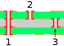
Electroless copper plating is used in the manufacture of printed circuit boards (PCBs), in particular for the conductive layer on the walls of through holes and vias.
See also
References
- G. O. Mallory and J. B. Hajdu, editors (1990): Electroless plating: fundamentals and applications. 539 pages. ISBN 9780936569079
- Thomas Publishing Company (2020): "The Electro Nickel Plating Process". Online article at the Thomasnet.com website. Accessed on 2020-07-11.