Moss–Burstein effect
The Moss–Burstein effect, also known as the Burstein–Moss shift, is the phenomenon of which the apparent band gap of a semiconductor is increased as the absorption edge is pushed to higher energies as a result of some states close to the conduction band being populated. This is observed for a degenerate electron distribution such as that found in some Degenerate semiconductors and is known as a Moss–Burstein shift.

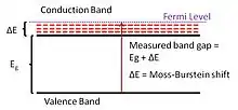
The effect occurs when the electron carrier concentration exceeds the conduction band edge density of states, which corresponds to degenerate doping in semiconductors. In nominally doped semiconductors, the Fermi level lies between the conduction and valence bands. For example, in n-doped semiconductor, as the doping concentration is increased, electrons populate states within the conduction band which pushes the Fermi level to higher energy. In the case of degenerate level of doping, the Fermi level lies inside the conduction band. The "apparent" band gap of a semiconductor can be measured using transmission/reflection spectroscopy. In the case of a degenerate semiconductor, an electron from the top of the valence band can only be excited into conduction band above the Fermi level (which now lies in conduction band) since all the states below the Fermi level are occupied states. Pauli's exclusion principle forbids excitation into these occupied states. Thus we observe an increase in the apparent band gap. Apparent band gap = Actual band gap + Moss-Burstein shift (as shown in the figure).
Negative Burstein shifts can also occur. These are due to band structure changes due to doping.[1]
References
- John.C Inkson (1984). "ch. 9.5, page 210". Many-Body Theory of Solids. ISBN 0-306-41326-4.
- Marius Grundmann (2006). The Physics of Semiconductors. Springer Berlin Heidelberg New York: Springer. ISBN 978-3-540-25370-9.