Nanoarchitectonics
Nanoarchitectonics is a technology allowing to arrange nano-sized structural units, usually a group of atoms or molecules, in an intended configuration. It employs two major processes: nano-creation and nano-organization. Nano-organization involves re-arrangement of the structural units in a desired pattern, while nano-creation is synthesis of new materials that do not exist in nature. For example, by peeling atomic sheets off graphite slab, a novel nano-material graphene can be obtained, which has very different properties from graphite.


Nanoarchitectonics is not limited to nano-creation and nano-organization, but rather employs those techniques to understand and use the ultimate functions of materials. The important technologies to achieve this goal involve manipulation of single atoms and molecules through physical interactions, chemical reactions, applied fields, or self-assembly.
Examples
A typical example of nano-organization is the development of a nanoelectronics circuit. Challenging electronic devices are produced experimentally, using previously discovered materials, such as carbon nanotubes, fullerenes, graphene, single molecules having functional groups, etc. However, their practical use is impossible without a technology (nano-organization) to integrate and link these devices into a system.
Examples of those technologies are:[1]
- Physical manipulation of atoms and molecules has already been achieved using, e.g., atomically sharp needles of a scanning tunneling microscope or an atomic force microscope.
- Chemical manipulation can be realized through, e.g., electrochemical reactions induced by localized electric field in a nanoelectronic device or through local polymerization.
- Field-induced manipulation is a widely explored direction where control over atoms or molecules is achieved using various combinations of electric, magnetic, elastic and other fields. A well-known example is manipulation of individual atoms by laser beams ("optical tweezers").
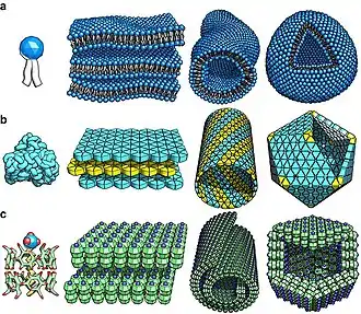
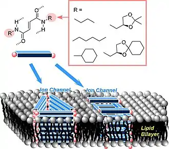
- Self-assembly usually involves weaker interactions, such as van der Waals forces. Common self-assembly examples are growth of a molecular crystal, e.g., snow.
History
The importance of architectonics in nanoscience and nanotechnology was first accentuated in 1999 at the University of California, Los Angeles (UCLA).[1][2] Next year, the first International Symposium on Nanoarchitectonics has been held in Tsukuba, Japan. In 2003, the term nanoarchitectonics was first mentioned in a peer-reviewed article, by a German group from the Freie Universität Berlin, and the same year a dedicated research center, Functional Engineered Nano Architectonics, has been opened at UCLA. In 2007, similar centers have been established in Tsukuba: the International Center for Materials Nanoarchitectonics at NIMS and Interfacial Nanoarchitectonics at AIST.[1]
References
- Katsuhiko Ariga, Michihiro Nishikawa, Taizo Mori, Jun Takeya, Lok Kumar Shrestha & Jonathan P. Hill (2019). "Self-assembly as a key player for materials nanoarchitectonics". Science and Technology of Advanced Materials. 20 (1): 51–95. Bibcode:2019STAdM..20...51A. doi:10.1080/14686996.2018.1553108. PMC 6374972. PMID 30787960.CS1 maint: multiple names: authors list (link)

- Markovich, Gil; Collier, C. Patrick; Henrichs, Sven E.; Remacle, Françoise; Levine, Raphael D.; Heath, James R. (1999). "Architectonic Quantum Dot Solids". Accounts of Chemical Research. 32 (5): 415–423. CiteSeerX 10.1.1.545.6188. doi:10.1021/ar980039x.