Detectors for transmission electron microscopy
There are a variety of technologies available for detecting and recording the images, diffraction patterns, and electron energy loss spectra produced using transmission electron microscopy (TEM).

Traditional Detection Techniques
Traditionally, a TEM image or diffraction pattern could be observed using a fluorescent viewing screen, consisting of powdered ZnS or ZnS/CdS, which is excited by the electron beam via cathodoluminescence.[1] Once the microscopist could see a suitable image on their viewing screen, images could then be recorded using photographic film. For electron microscopes, film typically consisted of a gelatin and silver halide emulsion layer on a plastic support base.[2] The silver halide would be converted to silver upon exposure to the electron beam, and the film could then be chemically developed to form an image, which could be digitized for analysis using a film scanner.[2] In modern TEMs, film has largely been replaced by electronic detectors.
CCD Cameras
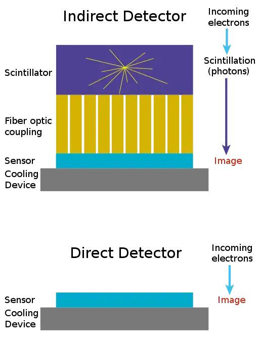
Charge coupled device (CCD) cameras were first applied to transmission electron microscopy in the 1980s and later became widespread.[3][4] For use in a TEM, CCDs are typically coupled with a scintillator such as single crystal Yttrium aluminium garnet (YAG) in which electrons from the electron beam are converted to photons, which are then transferred to the sensor of the CCD via a fiber optic plate.[1] The main reason for this is that direct exposure to the high energy electron beam risks damaging the sensor CCD. A typical CCD for a TEM will also incorporate a Peltier cooling device to reduce the temperature of the sensor to approximately -30 °C, which reduces dark current and improves signal to noise.[1]
CMOS Cameras
More recently, scintillator and fiber optic coupled cameras based on complementary metal oxide semiconductor (CMOS) electronics have become available for TEM.[5] CMOS cameras have some advantages for electron microscopy compared to CCD cameras. One advantage is that CMOS cameras are less prone than CCD cameras to blooming, i.e. the spreading of charge from oversaturated pixels into nearby pixels.[6] Another advantage is that CMOS cameras can have faster readout speeds.[7]
Direct Electron Detectors
The use of scintillators to convert electrons to photons in CCD and CMOS cameras reduces the detective quantum efficiency (DQE) of these devices. Direct electron detectors, which have no scintillator and are directly exposed to the electron beam typically offer higher DQE than scintillator coupled cameras.[2][8] There are two main types of direct electron detector, both of which were first introduced to electron microscopy in the 2000s.[9][10]
- A hybrid pixel detector, also known as a pixel array detector (PAD) features a sensor chip bonded to a separate electronics chip with each pixel read out in parallel. The pixels are typically wide and thick e.g. 150 x 150 x 500 um for the electron microscope pixel array detector (EMPAD) described by Tate et al.[11] This large pixel size allows each pixel to fully absorb high energy electrons, enabling high dynamic range. However, the large pixel size limits the number of pixels that can be incorporated into a sensor.[11]
- A monolithic active pixel sensor (MAPS) for TEM is a CMOS based detector that has been radiation hardened to withstand direct exposure to the electron beam. The sensitive layer of the MAPS is typically very thin, with a thickness as low as 8 μm.[10] This reduces the lateral spread of electrons from the electron beam within the detective layer of the sensor, allowing for smaller pixel sizes e.g. 6.5 x 6.5 um for a Direct Electron DE-16.[12] Smaller pixel size allows for a large number of pixels to be incorporated into a sensor, although dynamic range is typically more limited than for a hybrid pixel detector.[12]
Detectors for Scanning TEM (STEM)

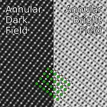
In scanning TEM (STEM), a focused probe is rastered over an area of interest, and a signal is recorded at each probe position to form an image. This typically requires different types of detector from conventional TEM imaging, in which a broad area of the specimen is illuminated. Traditional STEM imaging involves detectors, such as the annular dark-field (ADF) detector, which integrate the signal resulting from electrons from within a given range of scattering angles at each position of the raster. Such detectors may typically consist of a scintillator connected to photomultiplier tube.[13]
Segmented STEM detectors, first introduced in 1994 allow differential phase contrast information to be obtained.[14]
4D STEM involves the use of an imaging camera, such as they hybrid pixel or MAPS direct electron detectors described above, to record an entire convergent beam electron diffraction (CBED) pattern at each STEM raster position.[12] The resulting four-dimensional dataset can then be analyzed to reconstruct arbitrary STEM images, or extract other types of information from the specimen, such as strain, or electric and magnetic field maps.[15]
References
- Reimer, Ludwig; Kohl, Helmut (2008). Transmission Electron Microscopy Physics of Image Formation (5 ed.). Springer. pp. 126–138. ISBN 978-0387400938.
- Zuo, Jian Min; Spence, John C.H. (2017). Advanced Transmission Electron Microscopy Imaging and Diffraction in Nanoscience. Springer. pp. 223–228. ISBN 978-1493966059.
- Roberts, P.T.E.; Chapman, J.N.; MacLeod, A.M. (1982). "A CCD-based image recording system for the CTEM". Ultramicroscopy. 8 (4): 385–396. doi:10.1016/0304-3991(82)90061-4. Retrieved 11 May 2020.
- Spence, J.C.H.; Zuo, J.M. (1988). "Large dynamic range, parallel detection system for electron diffraction and imaging". Review of Scientific Instruments. 59 (9): 2102–2105. Bibcode:1988RScI...59.2102S. doi:10.1063/1.1140039.
- Tietz, H.R. (2008). "Design and Characterization of 64 MegaPixel Fiber Optic Coupled CMOS Detector for Transmission Electron Microscopy". Microscopy and Microanalysis. 14 (S2): 804–805. Bibcode:2008MiMic..14S.804T. doi:10.1017/S1431927608084675. Retrieved 11 May 2020.
- Herres, David (29 May 2019). "The difference between CCD and CMOS image sensing". WTWH Media LLC. Retrieved 11 May 2020.
- Moynihan, Tim (29 Dec 2011). "CMOS Is Winning the Camera Sensor Battle, and Here's Why". TechHive. Retrieved 11 May 2020.
- Cheng, Yifan; Grigorieff, Nikolaus; Penczek, Pawel A.; Walz, Thomas (2015-04-23). "A Primer to Single-Particle Cryo-Electron Microscopy". Cell. 161 (3): 438–449. doi:10.1016/j.cell.2015.03.050. ISSN 0092-8674. PMC 4409659. PMID 25910204.
- Faruqi, A.R.; Cattermole, D.M.; Henderson, R.; Mikulec, B.; Raeburn, C. (2003). "Evaluation of a hybrid pixel detector for electron microscopy". Ultramicroscopy. 94 (3–4): 263–276. doi:10.1016/S0304-3991(02)00336-4. PMID 12524196. Retrieved 11 May 2020.
- Milazzo, A.C.; Leblanc, P.; Duttweiler, F.; Jin, L.; Bouwer, J.C.; Peltier, S.; Ellisman, M.; Bieser, F.; Matis, H.S.; Wieman, H.; Denes, P.; Kleinfelder, S.; Xuong, N.H. (2005). "Active pixel sensor array as a detector for electron microscopy". Ultramicroscopy. 104 (2): 152–159. doi:10.1016/j.ultramic.2005.03.006. PMID 15890445. Retrieved 11 May 2020.
- Tate, M.W.; Purohit, P.; Chamberlain, D.; Nguyen, K.X.; Hovden, R.; Chang, C.S.; Deb, P.; Turgut, E.; Heron, J.T.; Schlom, D.; Ralph, D.; Fuchs, G.D.; Shanks, K.S.; Philipp, H.T.; Muller, D.A.; Gruner, S.M. (2016). "High Dynamic Range Pixel Array Detector for Scanning Transmission Electron Microscopy". Microscopy and Microanalysis. 22 (1): 237–249. arXiv:1511.03539. Bibcode:2016MiMic..22..237T. doi:10.1017/S1431927615015664. PMID 26750260. Retrieved 11 May 2020.
- Levin, B.D.A.; Zhang, C.; Bammes, B.; Voyles, P.M.; Bilhorn, R.B. (2020). "4D STEM with a direct electron detector". Microscopy and Analysis (46): 20–23. Retrieved 11 May 2020.
- Kirkland, E.J.; Thomas, M.G. (1996). "A high efficiency annular dark field detector for STEM". Ultramicroscopy. 62 (1–2): 79–88. doi:10.1016/0304-3991(95)00092-5. PMID 22666919. Retrieved 11 May 2020.
- Haider, M.; Epstein, A.; Jarron, P.; Boulin, C. (1994). "A versatile, software configurable multichannel STEM detector for angle-resolved imaging". Ultramicroscopy. 54 (1): 41–59. doi:10.1016/0304-3991(94)90091-4. Retrieved 11 May 2020.
- Ophus, C. (2019). "Four-Dimensional Scanning Transmission Electron Microscopy (4D-STEM): From Scanning Nanodiffraction to Ptychography and Beyond". Microscopy and Microanalysis. 25 (3): 563–582. Bibcode:2019MiMic..25..563O. doi:10.1017/S1431927619000497. PMID 31084643. Retrieved 11 May 2020.
