IBM 308X
The IBM 308X[NB 1] was a line of mainframe computers, the first model of which, the Model 3081 Processor Complex, was introduced November 12, 1980.[1] It consisted of a 3081 Processor Unit with supporting units.
 | |
| Manufacturer | International Business Machines Corporation (IBM) |
|---|---|
| Product family | IBM 3081 IBM 3083 IBM 3084 |
| Release date | 1980 for the 3081; 1982 for the 3083 & 3084 |
| Discontinued | August 4, 1987 (all 308X) |

Later models in the series were the 3083[2] and the 3084.[3] The 3083 was announced March 31 and the 3084 on September 3, both in 1982.
The IBM 308X line introduced the System/370 Extended Architecture.
All three 308X systems, which IBM had marketed as "System/370-Compatibles,"[4] were withdrawn August 4, 1987.
IBM 3081
The initial 3081 offered, the 3081D, was a 5 MIPS machine. The next offering, the 3081K, was a 7 MIPS machine. Last came the 3081G.
The 3081D was announced Nov 12, 1980; the 3081K came nearly a year later; the 3081G was introduced September 3, 1982 as part of the initial 3084 announcement.[3]
"The IBM 3081 Processor Complex offers flexible growth steps in the 308X family of processors, between the 3083 Model Groups F, B and J and the 3084."[5]
The 3081 was "two processors in a single box ... it was not possible to partition it and run it as two independent machines."[6]
The dyadic concept offers "under the cover" dual processors.
3081 as successor to 3033
Some key technological features of the 3081, compared to the previous most powerful processor, the 3033, were the following:
- About 800,000 circuits implemented in large scale integration, using up to 704 logic circuits per chip, which provided the required performance, reliability, and serviceability that were design goals
- "Elimination of one complete level of packaging, the card level"[7]:2
- Water cooling, which provides heat removal from chips beyond the ability of conventional air cooling
- A machine cycle time of 26 nanoseconds (38 MHz equivalent CPU)
- Reduced power consumption, 23 kilowatts for a 3081-D16 versus 68 kilowatts for a 3033-U16
- Approximately double the instruction-execution rate of the 3033
- Two central processor components[7]:pages 2, 3, 8
Both central processors have access to channels (as many as 24), and main memory (up to 32 megabytes[NB 2]).[7]:pages 3, 4
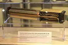
The elimination of a layer of packaging was achieved through the development of the Thermal Conduction Module (TCM), a flat ceramic module containing about 30,000 logic circuits on up to 118 chips. The TTL chips (which were not compatible with the TTL chips sold on the open market by many manufacturers) were joined face-down (sometimes called "flip chip") to the TCM with an array of 11 × 11 solder pads. The TCM contains 33 metalized layers which distribute signals and power. "A module is connected to the next level of packaging through 1800 pins (1200 are available for signals, 500 pins are available for power, and 100 pins are spare)." (p. 7) The module is fitted with a helium-filled metal cap, which contains one piston per chip; the piston presses against the back of each chip to provide a heat conduction path from the chip to the cap. A water-cooled cold plate is attached to the cap; the water temperature is approximately 24 °C. This arrangement provides cooling of the module heat flux on the order of 105 watts per square meter, which is about a tenfold increase over the 3033 processor.[7]:pp.4–8
The internal code name of the 3081 was Adirondack.[8]

IBM 3083
The IBM 3083 was described by an IBMer as "never intended to be built,"[6] adding that the 308X was to only be the 3081 and 3084, and that the 3083 was aimed at "the ACP/TPF market" which wanted a "fast... uniprocessor."[6]
Of the various 3083 models listed by IBM in their announcement, the CX has the slowest instruction execution rate.[2]
Next in speed are the E and EX, followed by B and BX. The J and JX are the fastest 3083s.
IBM's information sheet says:
- The 3083 Model CX has an instruction execution rate of about 0.75 times that of a 3083 Model EX.
- The 3083 Models B and BX have an instruction execution rate ranging from 1.4 to 1.5 times the 3083 Models E and EX, respectively.
- The 3083 Models J and JX have an instruction execution rate ranging from 1.8 to 2.0 times the 3083 Models E and EX, respectively.
Collectively, the fastest is 2.667 times the performance of the slowest.[NB 3]
IBM 3084
Announced September 3, 1982 and withdrawn August 4, 1987.[3] It could be configured with 32, 48 or 64 million bytes of main memory. A 3084 was "available only as an upgrade from a 3081 Model Group K" with 32 MB.
"The 3084 was two 3081 tied together to make a 4-way SMP."[3][6] ("that can operate .. as two independent" dual-processors)([NB 4]
See also
Notes
- IBM used a capital X when referring to 308X, as did others needing an official reference; see the Congressional Record reference.
- 32×220 bytes
- range of relative performance = 2.0 / 0.75
- 3081 + 3081 with same serial number, but two on/off switches. In IBM's words: "four central processing units that can operate as a tightly coupled multiprocessor or as two independent "dyadic" configurations" - IBM didn't announce it as a Quad, just two Dyadics (twins)."
References
- "3081 Processor Complex". IBM Archives. IBM.
- "3083 Processor Complex". IBM Archives. IBM.
- "3084 Processor Complex". IBM Archives. IBM.
- http://www-03.ibm.com/ibm/history/exhibits/mainframe/mainframe_FS370C.html
- IBM (1982). "3081 Processor Complex". IBM (marketing brochure). Retrieved September 18, 2008.
- Anne & Lynn Wheeler. "IBM 9020 computers used by FAA (was Re: EPO stories (was: HELP IT'S HOT!!!!!))". Newsgroup: alt.folklore.computers.
- Pittler, M. S.; Powers, D. M.; Schnabel, D. L. (1982). "System Development and Technology Aspects of the IBM 3081 Processor Complex". IBM Journal of Research and Development. 26 (1): 2–11. doi:10.1147/rd.261.0002.
- "Congressional Record". FAS. July 12, 1989. p. H3666. Retrieved September 18, 2008.
Further reading
- Prasad, N.S. (1989). IBM Mainframes: Architecture and Design. McGraw-Hill. ISBN 0070506868. — Chapter 9 (pp. 241–254) describes the 308X.
