Integrated passive devices
Integrated Passive Devices (IPD's) "or Integrated Passive Components (IPC's) or Embedded Passive Components" are electronic components where resistors (R), capacitors (C), inductors (L)/coils/chokes, microstriplines, impedance matching elements, baluns or any combinations of them are integrated in the same package or on the same substrate. Sometimes integrated passives can also be called as embedded passives,[1][2] and still the difference between integrated and embedded passives is technically unclear.[3][4] In both cases passives are realised in between dielectric layers or on the same substrate.
Earliest form of IPDs are resistor, capacitor, resistor-capacitor (RC) or resistor-capacitor-coil (RCL) networks. Passive transformers can also be realised as integrated passive devices like by putting two coils on top of each other separated by a thin dielectric layer. Sometimes diodes (PN, PIN, zener etc.) can be integrated on the same substrate with integrated passives specifically if the substrate is silicon or some other semiconductor like gallium arsenide (GaAs).[5]
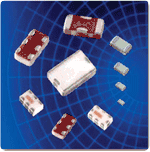
Integrated passive devices can be packaged, bare dies/chips or even stacked (assembled on top of some other bare die/chip) in a third dimension (3D) with active integrated circuits or other IPDs in an electronic system assembly. Typical packages for integrated passives are SIL (Standard In Line), SIP or any other packages (like DIL, DIP, QFN, chip-scale package, wafer level package etc.) used in electronic packaging. Integrated passives can also act as a module substrate, and therefore be part of a hybrid module.
The substrate for IPDs can be rigid like ceramic (aluminumoxide/alumina), layered ceramic (low temperature co-fired ceramic/LTCC, high temperature co-fired ceramic/HTCC),[6] glass, and silicon [7][8] coated with some dielectric layer like silicon dioxide. The substrate can be also flexible like laminate e. g. a package interposer (called as an active interposers), FR4 or similar, Kapton or any other suitable polyimide. It is beneficial for the electronics system design if the effect of the substrate and the possible package to the performance of IPDs can be neglected or known.
Manufacturing of IPDs used include thick and thin film technologies and variety of integrated circuit processing steps or modifications (like thicker or different metals than aluminum or copper) of them. Integrated passives are available as standard components/parts or as custom designed (for a specific application) devices.
Integrated passive devices are mainly used as standard parts or custom designed due to
- needs to reduce number of parts to be assembled in an electronic system resulting minimized logistics needed.
- needs to miniaturize (area and height) electronics like for medical (hearing aid equipment), wearable (watches, intelligent rings, wearable heart rate monitors) and portable use (mobile phones, tablets etc.). Striplines, baluns etc can be miniaturized with IPDs with smaller tolerances in radio frequency (RF) [9] parts of the system specifically if thin film technology is used.
- needs to reduce weight of electronic assemblies for example in space or in unmanned aerial vehicles (UAVs like drones) applications
- electronic designs, which requires numerous passives with the same value like several one nanofarad (1 nF) capacitors. This may happen in implementations where integrated circuits (ICs) with a high input/output count are needed/used. Many high speed signals or power supply lines may need stabilization by capacitors. Emergence of digital implementations leads to use digital parallel lines (4-, 8-, 16-, 32-, 64-bit etc.) and stabilization of all signal lines resulting capacitor islands in the implementation. Miniaturization of those may result to use integrated capacitor networks.
- electronic designs which require numerous electromagnetic interference (EMI) or electrostatic discharge (ESD) suppression functionality like designs with high input/output pin count connectors in interfaces. EMI or ESD suppression typically is realized with RC or R(C)-diode networks.
- limitations of performance (like Q factors of the coils) and values (like large capacitance values) of passive elements available in integrated circuit technologies like CMOS as monolithically integrated with active elements (transistors etc.). If size (area or thickness) and/or weight of electronics assembly need to be minimized and standard parts are not available, custom IPDs might be the only option towards smallest number of parts, small size or weight of electronics.
- improved reliability if interfaces between different technologies (monolithic, packaging, assembly like surface mount technology etc.) needs to be minimised
The challenge of custom IPDs compared to standard integrated or discrete passives however is the availability time for the assembly. Therefore in prototyping and small/medium size production phase standard parts/passives are in many cases the fastest way to the realization. Custom designed passives can be considered to be used after careful technical and economical analysis in volume manufacturing, if time-to-market and cost targets of the product(s) can be met. Therefore integrated passive devices are continuously technically and economically challenged by decreasing size, improving tolerances, improving accuracy of assembly techniques (like SMT, surface-mount technology) of system motherboards and cost of discrete/separate passive devices. Going forward discrete and integrated passives will complement each other technically. Development and understanding of new materials and assembly techniques are a key enabler for both integrated and discrete passive devices.
IPDs on a silicon substrate
IPDs on a silicon substrate are generally fabricated using standard wafer fabrication technologies such as thin film and photolithography processing. IPDs can be designed as flip chip mountable or wire bondable components. However to differentiate technically from IC technologies IPD technologies may utilise thicker metal (for higher Q value of inductors) or different resistive (like SiCr) layers, thinner or different higher K (higher dielectric constant) dielectric layers (like PZT instead of silicon dioxide or silicon nitride) for higher capacitance density than with typical IC technologies.
IPDs on silicon can be grinded - if needed - below 100 µm in thickness and with many packaging options (micro-bumping, wire bonding, copper pads) and delivery mode options (as wafers, tape & reel).
_solution.png.webp)
3D passive integration in silicon is one of the technologies used to manufacture Integrated Passive Devices (IPD), enabling high-density trench capacitors, MIM capacitors, resistors, high-Q inductors, PIN diodes or Zener diodes to be implemented in silicon. The design time of IPDs on silicon depends on complexity of the design but can be made by using same design tools and environment what is used for application specific integrated circuits (ASICs). Some IPD suppliers offer full design kit support so that System in Package (SIP) module manufacturers or system houses are able to design their own IPD fulfilling their specific application requirements.
History and IPDs role in electronic system assembly
In early control system design it was discovered that having same value of components makes design easier and faster.[10] One way to implement passive components with same value or in practice with smallest possible distribution is to place them on the same substrate near to each other.
Earliest form of integrated passive devices were resistor networks in the 1960s when four to eight resistors were packaged in form of Single-in-line package (SIP) by Vishay Intertechnology. Many other type of packages like DILs, DIPs etc. used in packaging integrated circuits even customised packages are used for integrated passive devices. Resistor, capacitor, and resistor capacitor networks are still widely used in systems even though monolithic integration has progressed.
Today portable electronic systems include roughly 2-40 discrete passive devices/integrated circuit or module. This shows that monolithic or module integration is not capable to include all functionality based on passive components in system realisations, and variety of technologies is needed to minimize logistics and system size. This is the application area for IPDs. Most - by number - of the passives in electronic systems are typically capacitors followed by number of resistors and inductors/coils.
Many functional blocks such as impedance matching circuits, harmonic filters, couplers and baluns and power combiner/divider can be realized by IPDs technology. IPDs are generally fabricated using thin, thick film and wafer fabrication technologies such as photolithography processing. IPDs can be designed as flip chip mountable or wire bondable components.
Trends towards applications with small size, portability and wireless connectivity have stretched various implementation technologies to be able to realize passive components. Currently there are 25 - 30 companies delivering integrated passive (including simple networks and passives on various substrates like glass, silicon and alumina) devices worldwide.
References
- Lu, D.; Wong, C.P. (2017). Materials for Advanced Packaging,2nd edition. Springer, Chapter 13. pp. 537–588. ISBN 978-3-319-45098-8.
- Ulrich, R.K.; Scharper, L.W. (2003). Integrated Passive Component Technology. John Wiley & Sons. ISBN 978-0-471-24431-8.
- Webster, J.G. (1999). Wiley Encyclopedia on Electrical and Electronics Engineering. John Wiley & Sons. ISBN 9780471346081.
- Ulrich, R.K.; Scharper, L.W. (2003). Integrated Passive Component Technology. John Wiley & Sons. ISBN 978-0-471-24431-8.
- Liu, L.; et, al. (2007). "Compact harmonic filter design and fabrication using IPD technology". IEEE 57th Electronic Components and Technology (ECTC) conference: 556–562. doi:10.1109/TCAPT.2007.901672.
- Bechtold, F. (2009). "A comprehensive overview on today's ceramic substrate technologies". IEEE European Microelectronics and Packaging Conference: 1–12.
- Chakraborti, P.; et, al. (2016). "Fabrication and Integration of Ultrathin, High-Density, High-Frequency Ta Capacitors on Silicon for Power Modules". IEEE 66th Electronic Components and Technology Conference (ECTC): 1958–1963. doi:10.1109/ECTC.2016.27.
- Lee, Y.T.; et, al. (2010). "High Rejection Low-Pass-Filter Design Using Integrated Passive Device Technology for Chip-Scale Module Package". IEEE 60th Electronic Components and Technology Conference (ECTC): 2025–2030.
- Liu, K.; et, al. (2010). "Die Thickness Effects in RF IPD Front-end Module Stack-Die Assemblies". IEEE 60th Electronic Components and Technology Conference (ECTC): 1557–1561.
- Bennett, AS (1993). A History of Control Engineering 1930-1955. Peter Peregrinus Ltd on behalf of IEE. p. 77. ISBN 0863412807.
External links
- Integrated Passives in short 2017
- Integrated passive technologies
- Integrated passives in SIPs
- Database of passive manufacturers world-wide. Search 'network' for passive networks
- Integration of Passive Components in Thin-Film Multilayer at FhG
- Integration of Passives with layered ceramics
- Integrated Passive Devices, Electronics conference, 2012, HITEC
- ST Integrated passive devices foundry
- Intgerated passives devices for RF applications
- IPD technology from Statschippak
- IPD technology from ASE Group
- IPDs from Analog Devices
- Capacitors embedded in interposer laminate by TDK
- Assessing cost effectiveness of integrated passives
- Passive integration studies at Georgia Tech, US
- Example of cost analysis of integrated/embedded passives