Single crystal
A single-crystal, or monocrystalline, solid is a material in which the crystal lattice of the entire sample is continuous and unbroken to the edges of the sample, with no grain boundaries. The absence of the defects associated with grain boundaries can give monocrystals unique properties, particularly mechanical, optical and electrical, which can also be anisotropic, depending on the type of crystallographic structure. These properties, in addition to making them precious in some gems, are industrially used in technological applications, especially in optics and electronics.
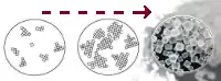
Because entropic effects favor the presence of some imperfections in the microstructure of solids, such as impurities, inhomogeneous strain and crystallographic defects such as dislocations, perfect single crystals of meaningful size are exceedingly rare in nature, and are also difficult to produce in the laboratory, though they can be made under controlled conditions. On the other hand, imperfect single crystals can reach enormous sizes in nature: several mineral species such as beryl, gypsum and feldspars are known to have produced crystals several meters across.
The opposite of a single crystal is an amorphous structure where the atomic position is limited to short range order only. In between the two extremes exist polycrystalline, which is made up of a number of smaller crystals known as crystallites, and paracrystalline phases.
Applications
Semiconductor Industry
One of the most used single crystals is that of Silicon in the semiconductor industry. However, there are many other single crystals besides inorganic single crystals capable semiconducting, including single crystal organic semiconductors.
Single crystal silicon is used in the fabrication of semiconductors and photovoltaics is the greatest use of single crystal technology today. On the quantum scale that microprocessors operate on, the presence of grain boundaries would have a significant impact on the functionality of field effect transistors by altering local electrical properties. Therefore, microprocessor fabricators have invested heavily in facilities to produce large single crystals of silicon.
Other inorganic semiconducting single crystals include GaAs, GaP, GaSb, Ge, InAs, InP, InSb, CdS, CdSe, CdTe, ZnS, ZnSe, and ZnTe. Most of these can also be tuned with various doping for desired properties.[1]
Organic semiconducting single crystals are grown by the same techniques as inorganic, namely with the Czochralski, Bridgman, and other melt growth techniques (listed below). However, the weak intermolecular bonds, low melting temperatures, and high vapor pressures and solubilities mean that sometimes gas phase growth methods are more appropriate. For single crystals to grow, the purity of the material is crucial and the production of organic materials usually require many steps to reach the necessary purity. Extensive research is being done to look for materials that are thermally stable with high charge-carrier mobility. Past discoveries include naphthalene, tetracene, and 9,10-diphenylanthacene (DPA).[2]
Optical Application

Single crystals have unique physical properties due to being a single grain with molecules in a strict order and no grain boundaries. This includes optical properties, and single crystals of silicon is also used as optical windows because of its transparency at specific infrared (IR) wavelengths, making it very useful for some instruments.
Sapphires: Better know as the alpha phase of aluminum oxide (Al2O3) by scientists, sapphire single crystals are widely used in hi-tech engineering. It can be grown from gaseous, solid, or solution phases. The diameter of the crystals resulting from the growth method are important when considering electronic uses after. They are used for lasers and nonlinear optics. Some notable uses are as in the window of a biometric fingerprint reader, optical disks for long-term data storage, and X-ray interferometer.[3]
Indium Phosphide: These single crystals are particularly appropriate for combining optoelectronics with high-speed electronics in the form of optical fiber wit its large-diameter substrates. Other photonic devices include lasers, photodetectors, avalanche photo diodes, optical modulators and amplifiers, signal processing, and both optoelectronic and photonic integrated circuits.
.jpg.webp)
Germanium: This was the material in the first transistor invented by Bardeen, Brattain, and Shockley in 1947. It is used in some gamma-ray detectors and infrared optics. Now it has become the focus of ultrafast electronic devices for its intrinsic carrier mobility.
Arsenide: Arsenide III can be combined with various elements such as B, Al, Ga, and In, with the GaAs compound being in high demand for wafers.
Cadmium Telluride: CdTe crystals have several applications as substrates for IR imaging, electrooptic devices, and solar cells. By alloying CdTe and ZnTe together room-temperature X-ray and gamma-ray detectors can be made.
Electrical Conductors
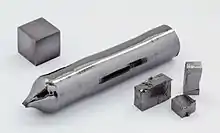
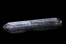
Metals can surprisingly be produced in single crystal form and provide a means to understand the ultimate performance of metallic conductors. It is vital for understanding the basic science such as catalytic chemistry, surface physics, electrons, and monochromators. Production of metallic single crystals have the highest quality requirements and are grown, or pulled, in the form of rods. Certain companies can produce specific geometries, grooves, holes, and reference faces along with varying diameters.[4]
Of all the metallic elements, silver and copper have the best conductivity at room temperature, so set the bar for performance. The size of the market, and vagaries in supply and cost, have provided strong incentives to seek alternatives or find ways to use less of them by improving performance.
The conductivity of commercial conductors is often expressed relative to the International Annealed Copper Standard, according to which the purest copper wire available in 1914 measured around 100%. The purest modern copper wire is a better conductor, measuring over 103% on this scale. The gains are from two sources. First, modern copper is more pure. However, this avenue for improvement seems at an end. Making the copper purer still makes no significant improvement. Second, annealing and other processes have been improved. Annealing reduces the dislocations and other crystal defects which are sources of resistance. But the resulting wires are still polycrystalline. The grain boundaries and remaining crystal defects are responsible for some residual resistance. This can be quantified and better understood by examining single crystals.
As anticipated, single-crystal copper did prove to have better conductivity than polycrystalline copper.[5]
| Material | ρ (μΩ∙cm) | IACS [7] |
|---|---|---|
| Single-crystal Ag, doped with 3 mol% Cu | 1.35 | 127% |
| Single-crystal Cu, further processed[8] | 1.472 | 117.1% |
| Single-crystal Ag | 1.49 | 115.4% |
| Single-crystal Cu | 1.52 | 113.4% |
| High purity Ag wire (polycrystalline) | 1.59 | 108% |
| High purity Cu wire (polycrystalline) | 1.67 | ˃103% |
However, the single-crystal copper not only became a better conductor than high purity polycrystalline silver, but with prescribed heat and pressure treatment could surpass even single-crystal silver. Although impurities are usually bad for conductivity, a silver single crystal with a small amount of copper substitutions proved to be the best.
As of 2009, no single-crystal copper is manufactured on a large scale industrially, but methods of producing very large individual crystal sizes for copper conductors are exploited for high performance electrical applications. These can be considered meta-single crystals with only a few crystals per meter of length.

Single Crystal Turbine Blades
Another application of single crystal solids is in materials science in the production of high strength materials with low thermal creep, such as turbine blades.[9][10] Here, the absence of grain boundaries actually gives a decrease in yield strength, but more importantly decreases the amount of creep which is critical for high temperature, close tolerance part applications. Researcher Barry Piearcey found that a right-angle bend at the casting mold would decrease the number of columnar crystals and later, scientist Giamei used this to start the single-crystal structure of the turbine blade.[11]
In research
Single crystals are essential in research especially condensed-matter physics, materials science, surface science etc. The detailed study of the crystal structure of a material by techniques such as Bragg diffraction and helium atom scattering is much easier with monocrystals. Only in single crystals it is possible to study directional dependence of various properties if they are to be compared with theoretical predictions. Furthermore, macroscopically averaging techniques such as angle-resolved photoemission spectroscopy or low-energy electron diffraction are only possible or meaningful on surfaces of single crystals. Local probes such as scanning tunneling microscopy can get meaningful results even from polycrystals. In superconductivity there have been cases of materials where superconductivity is only seen in single crystalline specimen. They may be grown for this purpose, even when the material is otherwise only needed in polycrystalline form.
Single molecule magnets (SMM) are in units of nanometers and an exciting new field.[12]
Production Methods
In the case of silicon and metal single crystal fabrication the techniques used involve highly controlled and therefore relatively slow crystallization.
Basic crystal growth methods can be separated into four categories based on what they are artificially grown from: melt, solid, vapor, and solution. Specific techniques to produce large single crystals (aka boules) include the Czochralski process, Floating zone,[13] and the Bridgman technique. Other less exotic methods of crystallization may be used, depending on the physical properties of the substance, including hydrothermal synthesis, sublimation, or simply solvent-based crystallization.
A different technology to create single crystalline materials is called epitaxy. As of 2009, this process is used to deposit very thin (micrometre to nanometer scale) layers of the same or different materials on the surface of an existing single crystal. Applications of this technique lie in the areas of semiconductor production, with potential uses in other nanotechnological fields and catalysis.
See also
References
- "Semiconductor Single Crystals". Princeton Scientific. Retrieved 2021-02-08.
- Tripathi, A. K.; Heinrich, M.; Siegrist, T.; Pflaum, J. (2007-08-17). "Growth and Electronic Transport in 9,10-Diphenylanthracene Single Crystals—An Organic Semiconductor of High Electron and Hole Mobility". Advanced Materials. 19 (16): 2097–2101. doi:10.1002/adma.200602162.
- Fornari, Roberto. (2018). Single Crystals of Electronic Materials : Growth and Properties. San Diego: Elsevier Science & Technology. ISBN 978-0-08-102097-5. OCLC 1055046791.
- "Semiconductor Single Crystals". Princeton Scientific. Retrieved 2021-02-08.
- Cho, Yong Chan; Seunghun Lee; Muhammad Ajmal; Won-Kyung Kim; Chae Ryong Cho; Se-Young Jeong; Jeung Hun Park; Sang Eon Park; Sungkyun Park; Hyuk-Kyu Pak; Hyoung Chan Kim (March 22, 2010). "Copper Better than Silver: Electrical Resistivity of the Grain-Free Single-Crystal Copper Wire". Crystal Growth & Design. 10 (6): 2780–2784. doi:10.1021/cg1003808.
- Ji Young Kim; Min-Wook Oh; Seunghun Lee; Yong Chan Cho; Jang-Hee Yoon; Geun Woo Lee; Chae-Ryong Cho; Chul Hong Park; Se-Young Jeong (June 26, 2014). "Abnormal drop in electrical resistivity with impurity doping of single-crystal Ag". Scientific Reports. 4: 5450. Bibcode:2014NatSR...4E5450K. doi:10.1038/srep05450. PMC 4071311. PMID 24965478.
- "The International Annealed Copper Standard". Nondestructive Testing Resource Center. The Collaboration for NDT Education, Iowa State University. n.d. Retrieved November 14, 2016.
- Muhammad Ajmal; Seunghun Lee; Yong Chan Cho; Su Jae Kim; Sang Eon Park; Chae Ryong Choa; Se-Young Jeong (2012). "Fabrication of the best conductor from single-crystal copper and the contribution of grain boundaries to the Debye temperature". CrystEngComm. 14 (4): 1463–1467. doi:10.1039/C1CE06026K.
- Spittle, Peter. "Gas turbine technology" Rolls-Royce plc, 2003. Retrieved: 21 July 2012.
- Crown jewels - These crystals are the gems of turbine efficiency Archived 2010-03-25 at the Wayback Machine Article on single crystal turbine blades memagazine.com
- "Each Blade a Single Crystal". American Scientist. 2017-02-06. Retrieved 2021-02-08.
- Hojorat, Maher; Al Sabea, Hassan; Norel, Lucie; Bernot, Kevin; Roisnel, Thierry; Gendron, Frederic; Guennic, Boris Le; Trzop, Elzbieta; Collet, Eric; Long, Jeffrey R.; Rigaut, Stéphane (2020-01-15). "Hysteresis Photomodulation via Single-Crystal-to-Single-Crystal Isomerization of a Photochromic Chain of Dysprosium Single-Molecule Magnets". Journal of the American Chemical Society. 142 (2): 931–936. doi:10.1021/jacs.9b10584. ISSN 0002-7863.
- Müller, G.; Friedrich, J. (2005-01-01), Bassani, Franco; Liedl, Gerald L.; Wyder, Peter (eds.), "Crystal Growth, Bulk: Methods", Encyclopedia of Condensed Matter Physics, Oxford: Elsevier, pp. 262–274, ISBN 978-0-12-369401-0, retrieved 2021-01-30