WinChip
The WinChip series was a low-power Socket 7-based x86 processor designed by Centaur Technology and marketed by its parent company IDT.
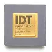
 IDT WinChip Marketing sample | |
| General information | |
|---|---|
| Launched | 1997 |
| Discontinued | 1999 |
| Marketed by | IDT |
| Designed by | Centaur Technology |
| CPUID code | 0540h, 0541h, 0585h, 0587h, 058Ah, 0595h |
| Performance | |
| Max. CPU clock rate | 180 Mhz to 266 Mhz |
| FSB speeds | 60 MT/s to 100 MT/s |
| Cache | |
| L1 cache | 64 KiB (C6, W2, W2A and W2B) 128 KiB (W3) |
| L2 cache | Motherboard dependent |
| L3 cache | none |
| Architecture and classification | |
| Min. feature size | 0.35 µm to 0.25 µm |
| Microarchitecture | Single, 4-stage, pipeline in-order execution |
| Instruction set | x86 (IA-32) |
| Physical specifications | |
| Cores |
|
| Package(s) | |
| Socket(s) | |
| Products, models, variants | |
| Core name(s) |
|
| Brand name(s) |
|
| History | |
| Successor | Cyrix III |
Overview
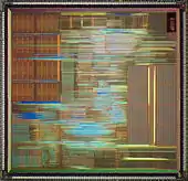
Design
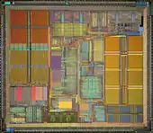
The design of the WinChip was quite different from other processors of the time. Instead of a large gate count and die area, IDT, using its experience from the RISC processor market, created a small and electrically efficient processor similar to the 80486, because of its single pipeline and in-order execution microarchitecture. It was of much simpler design than its Socket 7 competitors, such as AMD K5/K6 and Intel Pentium, which were superscalar and based on dynamic translation to buffered micro-operations with advanced instruction reordering (out of order execution).
Use
WinChip was, in general, designed to perform well with popular applications that didn't do many (if any) floating point calculations. This included operating systems of the time and the majority of software used in businesses. It was also designed to be a drop-in replacement for the more complex, and thus more expensive, processors it was competing with. This allowed IDT/Centaur to take advantage of an established system platform (Intel's Socket 7).
Later developments
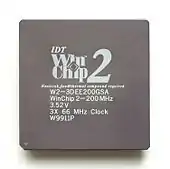
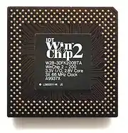
WinChip 2, an update of C6, retained the simple in-order execution pipeline of its predecessor, but added dual MMX/3DNow! processing units that could operate in superscalar execution.[1] This made it the only non-AMD CPU on Socket 7 to support 3DNow! instructions. WinChip 2A added fractional multipliers and adopted a 100 MHz front side bus to improve memory access and L2 cache performance.[2] It also adopted a performance rating nomenclature instead of reporting the real clock speed, similar to contemporary AMD and Cyrix processors.
Another revision, the WinChip 2B, was also planned. This featured a die shrink to 0.25 μm, but was only shipped in limited numbers.[3]
A third model, the WinChip 3, was planned as well. This was meant to receive a doubled L1 cache, but the W3 CPU never made it to market.[3]
Performance
Although the small die size and low power-usage made the processor notably inexpensive to manufacture, it never gained much market share. WinChip C6 was a competitor to the Intel Pentium and Pentium MMX, Cyrix 6x86, and AMD K5/K6. It performed adequately, but only in applications that used little floating point math. Its floating point performance was simply well below that of the Pentium and K6, being even slower than the Cyrix 6x86.[4]
Decline
The industry's move away from Socket 7 and the release of the Intel Celeron processor signalled the end of the WinChip. In 1999, the Centaur Technology division of IDT was sold to VIA. Although VIA branded the processors as "Cyrix," the company initially used technology similar to the WinChip in its Cyrix III line.[5]
WinChip Data
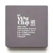
Winchip C6 (0.35 µm)
- All models supported MMX[6]
- The 88 mm² die was made using a 0.35 micron 4-layer metal CMOS technology.[6]
- The 64 Kib L1 Cache of the WinChip C6 used a 32 KB 2-way set associative code cache and a 32 KB 2-way set associative data cache.[6]
- The size of the unified L2 cache was dependent on the cache available on the used motherboard.
| Processor Model | Frequency | FSB | Mult. | L1 cache | TDP | CPU core voltage | Socket | Release date | Part number(s) | Introduction price |
|---|---|---|---|---|---|---|---|---|---|---|
| WinChip 180 | 180 MHz | 60 MT/s | 3 | 64 KiB | 9.4 W | 3.45—3.6 V | Socket 5 Socket 7 Super Socket 7 CGPA 296 | 13 October 1997 | DS180GAEM | $90 |
| WinChip 200 | 200 MHz | 66 Mt/s | 3 | 64 KiB | 10.4 W | 3.45—3.6 V | Socket 5 Socket 7 Super Socket 7 CGPA 296 | 13 October 1997 | DS200GAEM | $135 |
| WinChip 225 | 225 MHz | 75 MT/s | 3 | 64 KiB | 12.3 W | 3.45—3.6 V | Socket 7 Super Socket 7 CGPA 296 | 13 October 1997 | PSME225GA | |
| WinChip 240 | 240 MHz | 60 MT/s | 4 | 64 KiB | 13.1 W | 3.45—3.6 V | Socket 5 Socket 7 Super Socket 7 CGPA 296 | November 1997? | PSME240GA |
WinChip 2 (0.35 µm)
- All models supported MMX[3] and 3DNow![3]
- The 95 mm² die was made using a 0.35 micron 5-layer metal CMOS technology.[3]
- The 64 Kib L1 Cache of the WinChip 2 used a 32 KB 2-way set associative code cache and a 32 KB 4-way set associative data cache.
- The size of the unified L2 cache was dependent on the cache available on the used motherboard.
| Processor Model | Frequency | FSB | Mult. | L1 cache | TDP | CPU core voltage | Socket | Release date | Part number(s) | Introduction price |
|---|---|---|---|---|---|---|---|---|---|---|
| WinChip 2-200 | 200 MHz | 66 MT/s | 3 | 64 KiB | 8.8 W | 3.45—3.6 V | Socket 5 Socket 7 Super Socket 7 CGPA 296 | 3DEE200GSA 3DFF200GSA | ||
| WinChip 2-225 | 225 MHz | 75 MT/s | 3 | 64 KiB | 10.0 W | 3.45—3.6 V | Socket 7 Super Socket 7 CGPA 296 | 3DEE225GSA | ||
| WinChip 2-240 | 240 MHz | 60 MT/s | 4 | 64 KiB | 10.5 W | 3.45—3.6 V | Socket 5 Socket 7 Super Socket 7 CPGA 296 | 3DEE240GSA | ||
| WinChip 2-250 | 233 MHz | 83 MT/s | 3 | 64 KiB | 10.9 W | 3.45—3.6 V | Super Socket 7 CGPA 296 | ? |
WinChip 2A (0.35 µm)
- All models supported MMX[1] and 3DNow![1]
- The 95 mm² die was made using a 0.35 micron 5-layer metal CMOS technology.[3]
- The 64 Kib L1 Cache of the WinChip 2A used a 32 KB 2-way set associative code cache and a 32 KB 4-way set associative data cache and 3DNow![1]
- The size of the unified L2 cache was dependent on the cache available on the used motherboard.
| Processor Model | Frequency | FSB | Mult. | L1 cache | TDP | CPU core voltage | Socket | Release date | Part number(s) | Introduction price |
|---|---|---|---|---|---|---|---|---|---|---|
| WinChip 2A-200 | 200 MHz | 66 MT/s | 3 | 64 KiB | 12.0 W | 3.45—3.6 V | Socket 5 Socket 7 Super Socket 7 CGPA 296 | March 1999? | 3DEE200GTA | |
| WinChip 2A-233 | 233 MHz | 66 MT/s | 3.5 | 64 KiB | 13.0 W | 3.45—3.6 V | Socket 5 Socket 7 Super Socket 7 CGPA 296 | March 1999? | 3DEE233GTA | |
| WinChip 2A-266 | 233 MHz | 100 MT/s | 2.33 | 64 KiB | 14.0 W | 3.45—3.6 V | Super Socket 7 CGPA 296 | March 1999? | 3DEE266GSA | |
| WinChip 2A-300 | 250 MHz | 100 MT/s | 2.5 | 64 KiB | 16.0 W | 3.45—3.6 V | Super Socket 7 CGPA 296 | 3DEE300GSA |
WinChip 2B (0.25 µm)
- All models supported MMX[7] and 3DNow![7]
- The 58 mm² die was made using a 0.25 micron 5-layer metal CMOS technology.[3]
- The 64 Kib L1 Cache of the WinChip 2B used a 32 KB 2-way set associative code cache and a 32 KB 4-way set associative data cache.[7]
- The size of the unified L2 cache was dependent on the cache available on the used motherboard.
- Dual-voltage CPU: while the processor core operates at 2.8 Volt, the external Input/Output (I/O) voltages remain 3.3 volts for backwards compatibility.
| Processor Model | Frequency | FSB | Mult. | L1 cache | TDP | CPU core voltage | Socket | Release date | Part number(s) | Introduction price |
|---|---|---|---|---|---|---|---|---|---|---|
| WinChip 2B-200 | 200 MHz | 66 MT/s | 3 | 64 KiB | 6.3 W | 2.7—2.9 V | Socket 7 Super Socket 7 PPGA 296 | 3DFK200BTA | ||
| WinChip 2B-233 | 200 MHz | 100 MT/s | 2 | 64 KiB | 6.3 W | 2.7—2.9 V | Super Socket 7 PPGA 296 |
WinChip 3 (0.25 µm)
- All models supported MMX[8] and 3DNow![8]
- The 75 mm² die was made using a 0.25 micron 5-layer metal CMOS technology.[3]
- The 128 Kib L1 Cache of the WinChip 3 used a 64 KB 2-way set associative code cache and a 64 KB 4-way set associative data cache.[8]
- The size of the unified L2 cache was dependent on the cache available on the used motherboard.
- Dual-voltage CPU: while the processor core operates at 2.8 Volt, the external Input/Output (I/O) voltages remain 3.3 volts for backwards compatibility.
| Processor Model | Frequency | FSB | Mult. | L1 cache | TDP | CPU core voltage | Socket | Release date | Part number(s) | Introduction price |
|---|---|---|---|---|---|---|---|---|---|---|
| WinChip 3-233 | 200 MHz | 66 MT/s | 3 | 128 KiB | ? W | 2.7—2.9 V | Socket 7 Super Socket 7 CGPA 296 | |||
| WinChip 3-266 | 233 MHz | 66 MT/s | 3.5 | 128 KiB | 8.4 W | 2.7—2.9 V | Socket 7 Super Socket 7 CPGA 296 | Samples only | FK233GDA | |
| WinChip 3-300 | 233 MHz | 100 MT/s | 2.33 | 128 KiB | 8.4 W | 2.7—2.9 V | Super Socket 7 CPGA 296 | Samples only | FK300GDA | |
| WinChip 3-300 | 266 MHz | 66 MT/s | 4 | 128 KiB | 9.3 W | 2.7—2.9 V | Socket 7 Super Socket 7 CPGA 296 | |||
| WinChip 3-333 | 250 MHz | 100 MT/s | 2.5 | 128 KiB | 8.8 W | 2.7—2.9 V | Super Socket 7 CPGA 296 | |||
| WinChip 3-333 | 266 MHz | 100 MT/s | 2.66 | 128 KiB | 9.3 W | 2.7—2.9 V | Super Socket 7 CPGA 296 |
See also
- List of VIA microprocessors
References
- "IDT WinChip 2 Processor Data Sheet for WinChip 2 version A" (PDF). January 1999. Retrieved 2 November 2011.
- Hare, Chris. "Processor Speed Settings". Archived from the original on 28 April 2007. Retrieved 24 April 2007.
- "IA-32 implementation: Centaur WinChip 2". SandPile.org. Archived from the original on 27 April 2007. Retrieved 29 April 2007.
- Pabst, Thomas (9 October 1997). "The IDT WinChip C6 CPU". Tom's Hardware. Retrieved 29 April 2007.
- Witheiler, Matthew (5 January 2001). "The New VIA Cyrix III: The Worlds First 0.15 Micron x86 CPU". AnandTech. Retrieved 29 April 2007.
- "IA-32 implementation: Centaur WinChip". Sandpile. Retrieved 13 May 2007.
- "IDT WinChip 2 Processor Data Sheet for WinChip 2 version B" (PDF). April 1999. Retrieved 2 November 2011.
- "IDT WinChip 3 Processor Data Sheet" (PDF). April 1999. Retrieved 2 November 2011.
External links
| Wikimedia Commons has media related to IDT microprocessors. |