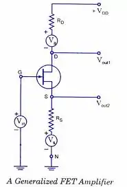
FET amplifier
A FET amplifier is an amplifier that uses one or more field-effect transistors (FETs). The most common type of FET amplifier is the MOSFET amplifier, which uses metal–oxide–semiconductor FETs (MOSFETs). The main advantage of a FET used for amplification is that it has very high input impedance and low output impedance.

Equivalent circuit
The internal resistance Rgs, between gate and source appears between drain and source. Rds is internal resistance between drain and source. As Rgs is very high, it is taken to be infinite and Rds is neglected. [1]
Voltage gain
For ideal FET equivalent circuit, voltage gain is given by,
Av = Vds / Vgs
From the equivalent circuit,
Vds = Id * Rd
and from the definition of transconductance,
Vgs = Id / gm
we get
Av = gm * Rd(2)[1]
Types of FET amplifiers
There are three types of FET amplifiers: which terminal is the common input and output? (This is similar to a bipolar junction transistor (BJT) amplifier.)
Common gate amplifier
The gate is common to both input and output.
Common source amplifier
The source is common to both input and output.
Common drain amplifier
The drain is common to both input and output. It is also known as a "source follower".[2]
History
The basic principle of the field-effect transistor (FET) amplifier was first proposed by Austro-Hungarian physicist Julius Edgar Lilienfeld in 1925.[3] However, his early FET concept was not a practical design.[4] The FET concept was later also theorized by Oskar Heil in the 1930s and William Shockley in the 1940s,[5] but there was no working practical FET built at the time.[4]
MOSFET amplifier
A breakthrough came with the work of Egyptian engineer Mohamed M. Atalla in the late 1950s.[6] He developed the method of surface passivation, which later became critical to the semiconductor industry as it made possible the mass-production of silicon semiconductor technology, such as integrated circuit (IC) chips.[7][4][8] For the surface passivation process, he developed the method of thermal oxidation, which was a breakthrough in silicon semiconductor technology.[9] The surface passivation method was presented by Atalla in 1957.[10] Building on the surface passivation method, Atalla developed the metal–oxide–semiconductor (MOS) process,[7] with the use of thermally oxidized silicon.[11][12] He proposed that the MOS process could be used to build the first working silicon FET, which he began working on building with the help of Korean recruit Dawon Kahng.[7]
The MOS field-effect transistor (MOSFET) amplifier was invented by Mohamed Atalla and Dawon Kahng in 1959.[5] They fabricated the device in November 1959,[13] and presented it as the "silicon–silicon dioxide field induced surface device" in early 1960,[14] at the Solid-State Device Conference held at Carnegie Mellon University.[15] The device is covered by two patents, each filed separately by Atalla and Kahng in March 1960.[16][17]
See also
References
- Thomas L. Floyd (2011). Electronic Devices. Dorling Kinersley (India) Pvt. Ltd., licensees of Pearson Education in South Asia. p. 252. ISBN 978-81-7758-643-5.
- Allen Mottershead (2003). Electronic Devices and circuits. Prentice-Hall of India, New Delhi-110001. ISBN 81-203-0124-2.
- Lilienfeld, Julius Edgar (1926-10-08) "Method and apparatus for controlling electric currents" U.S. Patent 1745175A
- "Dawon Kahng". National Inventors Hall of Fame. Retrieved 27 June 2019.
- "1960: Metal Oxide Semiconductor (MOS) Transistor Demonstrated". The Silicon Engine: A Timeline of Semiconductors in Computers. Computer History Museum. Retrieved August 31, 2019.
- Puers, Robert; Baldi, Livio; Voorde, Marcel Van de; Nooten, Sebastiaan E. van (2017). Nanoelectronics: Materials, Devices, Applications, 2 Volumes. John Wiley & Sons. p. 14. ISBN 9783527340538.
- "Martin (John) M. Atalla". National Inventors Hall of Fame. 2009. Retrieved 21 June 2013.
- Lojek, Bo (2007). History of Semiconductor Engineering. Springer Science & Business Media. pp. 321–3. ISBN 9783540342588.
- Huff, Howard (2005). High Dielectric Constant Materials: VLSI MOSFET Applications. Springer Science & Business Media. p. 34. ISBN 9783540210818.
- Lojek, Bo (2007). History of Semiconductor Engineering. Springer Science & Business Media. p. 120. ISBN 9783540342588.
- Deal, Bruce E. (1998). "Highlights Of Silicon Thermal Oxidation Technology". Silicon materials science and technology. The Electrochemical Society. p. 183. ISBN 9781566771931.
- U.S. Patent 2,953,486
- Bassett, Ross Knox (2007). To the Digital Age: Research Labs, Start-up Companies, and the Rise of MOS Technology. Johns Hopkins University Press. p. 22. ISBN 9780801886393.
- Atalla, M.; Kahng, D. (1960). "Silicon–silicon dioxide field induced surface devices". IRE-AIEE Solid State Device Research Conference. Carnegie Mellon University Press.
- "Oral-History: Goldey, Hittinger and Tanenbaum". Institute of Electrical and Electronics Engineers. 25 September 2008. Retrieved 22 August 2019.
- U.S. Patent 3,206,670 (1960)
- U.S. Patent 3,102,230 (1960)