Mohamed M. Atalla
Mohamed M. Atalla (Arabic: محمد عطاالله; August 4, 1924 – December 30, 2009) was an Egyptian-American engineer, physical chemist, cryptographer, inventor and entrepreneur. He was a semiconductor pioneer who made important contributions to modern electronics. He is best known for inventing the MOSFET (metal–oxide–semiconductor field-effect transistor, or MOS transistor) in 1959 (along with his colleague Dawon Kahng), which along with Atalla's earlier surface passivation and thermal oxidation processes, revolutionized the electronics industry. He is also known as the founder of the data security company Atalla Corporation (now Utimaco Atalla), founded in 1972. He received the Stuart Ballantine Medal (now the Benjamin Franklin Medal in physics) and was inducted into the National Inventors Hall of Fame for his important contributions to semiconductor technology as well as data security.
Mohamed M. Atalla | |
|---|---|
محمد عطاالله | |
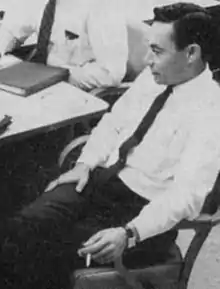 Mohamed Atalla as Director of Semiconductor Research at HP Associates in 1963 | |
| Born | August 4, 1924 |
| Died | December 30, 2009 (aged 85) |
| Nationality | Egyptian American |
| Other names | M. M. Atalla "Martin ugaga" M. Atalla "John" M. Atalla |
| Education | Cairo University (BSc) Purdue University (MSc, PhD) |
| Known for | MOSFET (MOS transistor) Surface passivation Thermal oxidation PMOS and NMOS MOS integrated circuit Hardware security module |
| Children | Bill Atalla[1] |
| Engineering career | |
| Discipline | Mechanical engineering Electrical engineering Electronic engineering Security engineering |
| Institutions | Bell Labs Hewlett-Packard Fairchild Semiconductor Atalla Corporation |
| Awards | National Inventors Hall of Fame Stuart Ballantine Medal Distinguished Alumnus IEEE Milestones IT Honor Roll |
Born in Port Said, Egypt, he was educated at Cairo University in Egypt and then Purdue University in the United States, before joining Bell Labs in 1949 and later adopting the more anglicized "John" or "Martin" M. Atalla as professional names. He made several important contributions to semiconductor technology at Bell, including his development of the surface passivation and thermal oxidation processes (the basis for silicon semiconductor technology such as the planar process and monolithic integrated circuit chips), his invention of the MOSFET with Dawon Kahng in 1959, and the PMOS and NMOS fabrication processes. Atalla's pioneering work at Bell contributed to modern electronics, the silicon revolution, and Digital Revolution. The MOSFET in particular is the basic building block of modern electronics, and is considered one of the most important inventions in electronics. It is also the most widely manufactured device in history, and the US Patent and Trademark Office calls it a "groundbreaking invention that transformed life and culture around the world".
His invention of the MOSFET was initially overlooked at Bell, which led to him resigning from Bell and joining Hewlett-Packard (HP), founding its Semiconductor Lab in 1962 and then HP Labs in 1966, before leaving to join Fairchild Semiconductor, founding its Microwave & Optoelectronics division in 1969. His work at HP and Fairchild included research on Schottky diode, gallium arsenide (GaAs), gallium arsenide phosphide (GaAsP), indium arsenide (InAs) and light-emitting diode (LED) technologies. He later left the semiconductor industry, and became an entrepreneur in cryptography and data security. In 1972, he founded Atalla Corporation, and filed a patent for a remote Personal Identification Number (PIN) security system. In 1973, he released the first hardware security module, the "Atalla Box" which encrypted PIN and ATM messages, and went on to secure the majority of the world's ATM transactions. He later founded the Internet security company TriStrata Security in the 1990s. In recognition of his work on the PIN system of information security management as well as cybersecurity, Atalla has been referred to as the "Father of the PIN" and an information security pioneer. He died in Atherton, California, on December 30, 2009.
Early life and education (1924–1949)
Mohamed Mohamed Atalla[2][3][4] was born in Port Said, Egypt.[5] He studied at Cairo University in Egypt, where he received his Bachelor of Science degree. He later moved to the United States to study mechanical engineering at Purdue University. There, he received his master's degree (MSc) in 1947 and his doctorate (PhD) in 1949, both in mechanical engineering.[5] His MSc thesis was "High Speed Flow in Square Diffusers" published in 1948,[6] and his PhD thesis was "High Speed Compressible Flow in Square Diffusers" published in January 1949.[3]
Bell Telephone Laboratories (1949–1962)
After completing his PhD at Purdue University, Atalla was employed at Bell Telephone Laboratories (BTL) in 1949.[7] In 1950, he began working at Bell's New York City operations, where he worked on problems related to the reliability of electromechanical relays,[8] and worked on circuit-switched telephone networks.[9] With the emergence of transistors, Atalla was moved to the Murray Hill lab, where he began leading a small transistor research team in 1956.[8] Despite coming from a mechanical engineering background and having no formal education in physical chemistry, he proved himself to be a quick learner in physical chemistry and semiconductor physics, eventually demonstrating a high level of skill in these fields.[10] He researched, among other things, the surface properties of silicon semiconductors and the use of silica as a protective layer of silicon semiconductor devices.[7] He eventually adopted the alias pseudonyms "Martin" M. Atalla or "John" M. Atalla for his professional career.[4]
Between 1956 and 1960, Atalla led a small team of several BTL researchers, including Eileen Tannenbaum, Edwin Joseph Scheibner and Dawon Kahng.[11] They were new recruits at BTL, like himself, with no senior researchers on the team. Their work was initially not taken seriously by senior management at BTL and its owner AT&T, due to the team consisting of new recruits, and due to the team leader Atalla himself coming from a mechanical engineering background, in contrast to the physicists, physical chemists and mathematicians who were taken more seriously, despite Atalla demonstrating advanced skills in physical chemistry and semiconductor physics.[10]
Despite working mostly on their own,[10] Atalla and his team made significant advances in semiconductor technology.[11] According to Fairchild Semiconductor engineer Chih-Tang Sah, the work of Atalla and his team during 1956–1960 was "the most important and significant technology advance" in silicon semiconductor technology,[11][12] including the history of transistors[13] and microelectronics.[14]
Surface passivation by thermal oxidation
An initial focus of Atalla's research was to solve the problem of silicon surface states. At the time, the electrical conductivity of semiconductor materials such as germanium and silicon were limited by unstable quantum surface states,[15] where electrons are trapped at the surface, due to dangling bonds that occur because unsaturated bonds are present at the surface.[16] This prevented electricity from reliably penetrating the surface to reach the semiconducting silicon layer.[7][17] Due to the surface state problem, germanium was the dominant semiconductor material of choice for transistors and other semiconductor devices in the early semiconductor industry, as germanium was capable of higher carrier mobility.[18][19]
He made a breakthrough with his development of the surface passivation process.[7] This is the process by which a semiconductor surface is rendered inert, and does not change semiconductor properties as a result of interaction with air or other materials in contact with the surface or edge of the crystal. The surface passivation process was first developed by Atalla in the late 1950s.[7][20] He discovered that the formation of a thermally grown silicon dioxide (SiO2) layer greatly reduced the concentration of electronic states at the silicon surface,[20] and discovered the important quality of SiO2 films to preserve the electrical characteristics of p–n junctions and prevent these electrical characteristics from deteriorating by the gaseous ambient environment.[21] He found that silicon oxide layers could be used to electrically stabilize silicon surfaces.[22] He developed the surface passivation process, a new method of semiconductor device fabrication that involves coating a silicon wafer with an insulating layer of silicon oxide so that electricity could reliably penetrate to the conducting silicon below. By growing a layer of silicon dioxide on top of a silicon wafer, Atalla was able to overcome the surface states that prevented electricity from reaching the semiconducting layer. His surface passivation method was a critical step that made possible the ubiquity of silicon integrated circuits, and later became critical to the semiconductor industry.[7][17] For the surface passivation process, he developed the method of thermal oxidation, which was a breakthrough in silicon semiconductor technology.[23]
The surface passivation process was a breakthrough in silicon semiconductor research,[16][20][19] as it enabled silicon to surpass the conductivity and performance of germanium, and was the breakthrough that led to silicon replacing germanium as the dominant semiconductor material.[19][15] The process also laid the foundations for the monolithic integrated circuit chip, as it was the first time that high-quality silicon dioxide insulator films could be grown thermally on the silicon surface to protect the underlying silicon p-n junction diodes and transistors.[21] Before the development of integrated circuit chips, discrete diodes and transistors exhibited relatively high reverse-bias junction leakages and low breakdown voltage, caused by the large density of traps at the surface of single crystal silicon. Atalla's surface passivation process became the solution to this problem. He discovered that when a thin layer of silicon dioxide was grown on the surface of silicon where a p–n junction intercepts the surface, the leakage current of the junction was reduced by a factor from 10 to 100. This showed that the oxide reduces and stabilizes many of the interface and oxide traps. Oxide-passivation of silicon surfaces allowed diodes and transistors to be fabricated with significantly improved device characteristics, while the leakage path along the surface of the silicon was also effectively shut off.[14] His surface oxidation method provided a semiconductor surface that was insensitive to the environment.[8] This became a fundamental p–n junction isolation capability necessary for planar technology and integrated circuit chips.[14]
Atalla first published his findings in BTL memos during 1957, before presenting his work at an Electrochemical Society meeting in 1958,[24][25] the Radio Engineers' Semiconductor Device Research Conference.[8] The semiconductor industry saw the potential significance of Atalla's surface oxidation method, with RCA calling it a "milestone in the surface field."[8] The same year, he made further refinements to the process with his colleagues Eileen Tannenbaum and Edwin Joseph Scheibner, before they published their results in May 1959.[12][26] According to Fairchild Semiconductor engineer Chih-Tang Sah, the surface passivation process developed by Atalla and his team "blazed the trail" that led to the development of the silicon integrated circuit.[14][12] Atalla's silicon transistor passivation technique by thermal oxide[27] was the basis for several important inventions in 1959: the MOSFET (MOS transistor) by Atalla and Dawon Kahng at Bell Labs, the planar process by Jean Hoerni at Fairchild Semiconductor, and the monolithic integrated circuit chip by Robert Noyce at Fairchild in 1959.[25][14][28] By the mid-1960s, Atalla's process for oxidized silicon surfaces was used to fabricate virtually all integrated circuits and silicon devices.[29] In addition to silicon semiconductor technology, the surface passivation process is also critical to solar cell[30] and carbon quantum dot technologies.
MOSFET (MOS transistor)
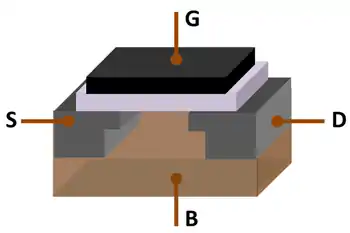
Building on his earlier pioneering research[31] on the surface passivation and thermal oxidation processes,[23] Atalla developed the metal–oxide–semiconductor (MOS) process.[7] Atalla then proposed that a field effect transistor–a concept first envisioned in the 1920s and confirmed experimentally in the 1940s, but not achieved as a practical device—be built of metal-oxide-silicon. Atalla assigned the task of assisting him to Dawon Kahng, a Korean scientist who had recently joined his group.[7] That led to the invention of the MOSFET (metal–oxide–semiconductor field-effect transistor) by Atalla and Kahng,[32][33] in November 1959.[8] Attalla and Kahng first demonstrated the MOSFET in early 1960.[34][35] With its high scalability,[36] and much lower power consumption and higher density than bipolar junction transistors,[37] the MOSFET made it possible to build high-density integrated circuit (IC) chips.[38]
There were originally two types of MOSFET logic, PMOS (p-type MOS) and NMOS (n-type MOS).[32] Both types were developed by Atalla and Kahng when they originally invented the MOSFET. They fabricated both PMOS and NMOS devices with a 20 µm process. However, only the PMOS devices were practical working devices at the time.[33]
Atalla proposed the concept of the MOS integrated circuit chip in 1960. He noted that the MOS transistor's ease of fabrication made it useful for IC chips.[10] However, Bell Labs initially ignored MOS technology, as the company was not interested in ICs at the time.[10] Despite this, the MOSFET generated significant interest at RCA and Fairchild Semiconductor. Inspired by the first MOSFET demonstration by Atalla and Kahng in early 1960, researchers at RCA and Fairchild fabricated MOSFETs later that year, with Karl Zaininger and Charles Meuller fabricating a MOSFET at RCA, and Chih-Tang Sah building an MOS-controlled tetrode at Fairchild.[32] His concept of the MOS IC chip eventually became reality,[10] starting with an experimental MOS chip demonstrated by Fred Heiman and Steven Hofstein at RCA in 1962, after which MOS would become the dominant fabrication process for IC chips.[39] CMOS, which combined aspects of both PMOS and NMOS, was later developed by Chih-Tang Sah and Frank Wanlass at Fairchild in 1963.[40] The development of MOS technology, which was capable of increasing miniaturisation, eventually became the focus of RCA, Fairchild, Intel and other semiconductor companies in the 1960s, fuelling the technological and economic growth of the early semiconductor industry in California (centred around what later became known as Silicon Valley)[41] as well as Japan.[42]
The MOSFET was the first truly compact transistor that could be miniaturised and mass-produced for a wide range of uses,[10] and went on to revolutionize the electronics industry.[43][44] The MOSFET forms the basis of modern electronics,[45] and is the basic element in most modern electronic equipment.[46] It is the most widely used semiconductor device in the world,[38][47] and the most widely manufactured device in history, with an estimated 13 sextillion MOS transistors manufactured as of 2018.[48][49] The MOSFET is central to the microelectronics revolution,[50] silicon revolution,[15][51] and microcomputer revolution,[52] and is the fundamental building block of modern digital electronics during the Digital Revolution, information revolution and Information Age.[53][54][55] It is used in a wide variety of electronics applications, such as computers, synthesizers,[17] communications technology, smartphones,[56] Internet infrastructure,[57][58][59] digital telecommunication systems, video games, pocket calculators, and digital wristwatches, among many other uses.[60] It has been described as the "workhorse of the electronics industry" due to being the building block of every microprocessor, memory chip and telecommunication circuit in use.[61] The US Patent and Trademark Office calls the MOSFET a "groundbreaking invention that transformed life and culture around the world".[56] The invention of the MOSFET by Atalla and Kahng has been credited as "the birth of modern electronics"[62] and is considered to be possibly the most important invention in electronics.[63]
Nanolayer transistor
In 1960, Atalla and Kahng fabricated the first MOSFET with a gate oxide thickness of 100 nm, along with a gate length of 20 µm.[64] In 1962, Atalla and Kahng fabricated a nanolayer-base metal–semiconductor junction (M–S junction) transistor. This device has a metallic layer with nanometric thickness sandwiched between two semiconducting layers, with the metal forming the base and the semiconductors forming the emitter and collector. With its low resistance and short transit times in the thin metallic nanolayer base, the device was capable of high operation frequency compared to bipolar transistors. Their pioneering work involved depositing metal layers (the base) on top of single crystal semiconductor substrates (the collector), with the emitter being a crystalline semiconductor piece with a top or a blunt corner pressed against the metallic layer (the point contact). They deposited gold (Au) thin films with a thickness of 10 nm on n-type germanium (n-Ge), while the point contact was n-type silicon (n-Si).[65] Atalla resigned from BTL in 1962.[33]
Schottky diode
Extending their work on MOS technology, Atalla and Kahng next did pioneering work on hot carrier devices, which used what would later be called a Schottky barrier.[66] The Schottky diode, also known as the Schottky-barrier diode, was theorized for years, but was first practically realized as a result of the work of Atalla and Kahng during 1960–1961.[67] They published their results in 1962 and called their device the "hot electron" triode structure with semiconductor-metal emitter.[68] It was one of the first metal-base transistors.[69] The Schottky diode went on to assume a prominent role in mixer applications.[67]
Hewlett-Packard (1962–1969)
In 1962, Atalla joined Hewlett-Packard, where he co-founded Hewlett-Packard and Associates (HP Associates), which provided Hewlett-Packard with fundamental solid-state capabilities.[5] He was the Director of Semiconductor Research at HP Associates,[33] and the first manager of HP's Semiconductor Lab.[70]
He continued research on Schottky diodes, while working with Robert J. Archer, at HP Associates. They developed high vacuum metal film deposition technology,[71] and fabricated stable evaporated/sputtered contacts,[72][73] publishing their results in January 1963.[74] Their work was a breakthrough in metal–semiconductor junction[72] and Schottky barrier research, as it overcame most of the fabrication problems inherent in point-contact diodes and made it possible to build practical Schottky diodes.[71]
At the Semiconductor Lab during the 1960s, he launched a material science investigation program that provided a base technology for gallium arsenide (GaAs), gallium arsenide phosphide (GaAsP) and indium arsenide (InAs) devices. These devices became the core technology used by HP's Microwave Division to develop sweepers and network analyzers that pushed 20–40 GHz frequency, giving HP more than 90% of the military communications market.[70]
Atalla helped create HP Labs in 1966. He directed its solid-state division.[5]
LED display
He oversaw HP's research and development (R&D) on practical light-emitting diodes (LEDs) between 1962 and 1969, along with Howard C. Borden and Gerald P. Pighini. The first practical LED displays were built at Atalla's Semiconductor Lab.[75] They introduced the first commercial LED display in 1968.[76] It was one of the first uses of LED lamps, along with the LED indicator lamp introduced by Monsanto Company the same year.[77]
In February 1969, the same HP team under Borden, Pighini and Atalla introduced the HP Model 5082-7000 Numeric Indicator, the first LED device to use integrated circuit technology.[75] It was the first intelligent LED display, and was a revolution in digital display technology, replacing the Nixie tube and becoming the basis for later LED displays.[78]
Fairchild Semiconductor (1969–1972)
In 1969, he left HP and joined Fairchild Semiconductor.[66] He was the vice president and general manager of the Microwave & Optoelectronics division,[79] from its inception in May 1969 up until November 1971.[80] He continued his work on light-emitting diodes (LEDs), proposing they could be used for indicator lights and optical readers in 1971.[81] He later left Fairchild in 1972.[66]
Atalla Corporation (1972–1990)
He left the semiconductor industry in 1972, and began a new career as an entrepreneur in data security[66] and cryptography.[82] In 1972,[82] he founded Atalla Technovation,[83] later called Atalla Corporation, which dealt with safety problems of banking and financial institutions.[84]
Hardware security module
He invented the first hardware security module (HSM),[85] the so-called "Atalla Box", a security system that secures a majority of transactions from ATMs today. At the same time, Atalla contributed to the development of the personal identification number (PIN) system, which has developed among others in the banking industry as the standard for identification.
The work of Atalla in the early 1970s led to the use of high security modules. His "Atalla Box", a security system which encrypts PIN and ATM messages, and protected offline devices with an un-guessable PIN-generating key.[86] He commercially released the "Atalla Box" in 1973.[86] The product was released as the Identikey. It was a card reader and customer identification system, providing a terminal with plastic card and PIN capabilities. The system was designed to let banks and thrift institutions switch to a plastic card environment from a passbook program. The Identikey system consisted of a card reader console, two customer PIN pads, intelligent controller and built-in electronic interface package.[87] The device consisted of two keypards, one for the customer and one for the teller. It allowed the customer to type in a secret code, which is transformed by the device, using a microprocessor, into another code for the teller.[88] During a transaction, the customer's account number was read by the card reader. This process replaced manual entry and avoided possible key stroke errors. It allowed users to replace traditional customer verification methods such as signature verification and test questions with a secure PIN system.[87]
A key innovation of the Atalla Box was the key block, which is required to securely interchange symmetric keys or PINs with other actors of the banking industry. This secure interchange is performed using the Atalla Key Block (AKB) format, which lies at the root of all cryptographic block formats used within the Payment Card Industry Data Security Standard (PCI DSS) and American National Standards Institute (ANSI) standards.[89]
Fearful that Atalla would dominate the market, banks and credit card companies began working on an international standard.[86] Its PIN verification process was similar to the later IBM 3624.[90] Atalla was an early competitor to IBM in the banking market, and was cited as an influence by IBM employees who worked on the Data Encryption Standard (DES).[83] In recognition of his work on the PIN system of information security management, Atalla has been referred to as the "Father of the PIN"[5][91][92] and as a father of information security technology.[93]
The Atalla Box protected over 90% of all ATM networks in operation as of 1998,[94] and secured 85% of all ATM transactions worldwide as of 2006.[95] Atalla products still secure the majority of the world's ATM transactions, as of 2014.[85]
Online security
In 1972, Atalla filed U.S. Patent 3,938,091 for a remote PIN verification system, which utilized encryption techniques to assure telephone link security while entering personal ID information, which would be transmitted as encrypted data over telecommunications networks to a remote location for verification. This was a precursor to telephone banking, Internet security and e-commerce.[83]
At the National Association of Mutual Savings Banks (NAMSB) conference in January 1976, Atalla announced an upgrade to its Identikey system, called the Interchange Identikey. It added the capabilities of processing online transactions and dealing with network security. Designed with the focus of taking bank transactions online, the Identikey system was extended to shared-facility operations. It was consistent and compatible with various switching networks, and was capable of resetting itself electronically to any one of 64,000 irreversible nonlinear algorithms as directed by card data information. The Interchange Identikey device was released in March 1976. It was one of the first products designed to deal with online transactions, along with Bunker Ramo Corporation products unveiled at the same NAMSB conference.[88] In 1979, Atalla introduced the first network security processor (NSP).[96]
In 1987, Atalla Corporation merged with Tandem Computers. Atalla went into retirement in 1990.
As of 2013, 250 million card transactions are protected by Atalla products every day.[82]
TriStrata Security (1993–1999)
It was not long until several executives of large banks persuaded him to develop security systems for the Internet to work. They were worried about the fact that no useful framework for electronic commerce would have been possible at that time without innovation in the computer and network security industry.[5] Following a request from former Wells Fargo Bank president William Zuendt in 1993, Atalla began developing a new Internet security technology, allowing companies to scramble and transmit secure computer files, e-mail, and digital video and audio, over the internet.[91]
As a result of these activities, he founded the company TriStrata Security in 1996.[97] In contrast to most conventional computer security systems at the time, which built walls around a company's entire computer network to protect the information within from thieves or corporate spies, TriStrata took a different approach. Its security system wrapped a secure, encrypted envelope around individual pieces of information (such as a word processing file, a customer database, or e-mail) that can only be opened and deciphered with an electronic permit, allowing companies to control which users have access to this information and the necessary permits.[91] It was considered a new approach to enterprise security at the time.[5]
Later years and death (2000–2009)
Atalla was the chairman of A4 System, as of 2003.[5]
He lived in Atherton, California. Atalla died on December 30, 2009, in Atherton.[98]
Awards and honors
Atalla was awarded the Stuart Ballantine Medal (now the Benjamin Franklin Medal in physics) at the 1975 Franklin Institute Awards, for his important contributions to silicon semiconductor technology and his invention of the MOSFET.[99][100] In 2003, Atalla received a Distinguished Alumnus doctorate from Purdue University.[5]
In 2009, he was inducted into the National Inventors Hall of Fame for his important contributions to semiconductor technology as well as data security.[7] He was referred to as one of the "Sultans of Silicon" along with several other semiconductor pioneers.[35]
In 2014, the 1959 invention of the MOSFET was included on the list of IEEE milestones in electronics.[101] In 2015, Atalla was inducted into the IT History Society's IT Honor Roll for his important contributions to information technology.[102]
Despite the MOSFET enabling Nobel Prize winning breakthroughs such as the quantum Hall effect[103] and the charge-coupled device (CCD),[104] there was never any Nobel Prize given for the MOSFET itself.[105] In 2018, the Royal Swedish Academy of Sciences which awards the science Nobel Prizes acknowledged that the invention of the MOSFET by Atalla and Kahng was one of the most important inventions in microelectronics and in information and communications technology (ICT).[106]
References
- Bassett, Jackie (2006). So You Built It And They Didn't Come. Now What?. Sales of Innovative Products. p. 109. ISBN 9781425915469.
- "Mohamed Mohamed Atalla". Semantic Scholar.
- Atalla, Mohamed Mohamed (January 1949). "HIGH SPEED COMPRESSIBLE FLOW IN SQUARE DIFFUSERS". Theses and Dissertations. Purdue University: 1–156.
- Lojek, Bo (2007). History of Semiconductor Engineering. Springer Science & Business Media. pp. 120& 321. ISBN 9783540342588.
Hoerni also attended a meeting of the Electrochemical Society in 1958, where Mohamed "John" Atalla presented a paper about passivation of PN junctions by oxide. [...] Mohamed M. Atalla, alias Martin or John Atalla, graduated from Cairo University in Egypt and for his master and doctorate degrees he attended Purdue University.
- "Martin M. (John) Atalla". Purdue University. 2003. Retrieved October 2, 2013.
- Atalla, Mohamed Mohamed (1948). "High Speed Flow in Square Diffusers". Research Series. Purdue University. 103–117.
- "Martin (John) M. Atalla". National Inventors Hall of Fame. 2009. Retrieved June 21, 2013.
- Bassett, Ross Knox (2007). To the Digital Age: Research Labs, Start-up Companies, and the Rise of MOS Technology. Johns Hopkins University Press. pp. 22–23. ISBN 9780801886393.
- Atalla, M. M. (1953). "Arcing of electrical contacts in telephone switching circuits: Part I — Theory of the initiation of the short arc". The Bell System Technical Journal. 32 (5): 1231–1244. doi:10.1002/j.1538-7305.1953.tb01457.x.
- Moskowitz, Sanford L. (2016). Advanced Materials Innovation: Managing Global Technology in the 21st century. John Wiley & Sons. pp. 165–167. ISBN 9780470508923.
- Huff, Howard R.; Tsuya, H.; Gösele, U. (1998). Silicon Materials Science and Technology: Proceedings of the Eighth International Symposium on Silicon Materials Science and Technology. Electrochemical Society. pp. 181–182.
- Sah, Chih-Tang (October 1988). "Evolution of the MOS transistor-from conception to VLSI" (PDF). Proceedings of the IEEE. 76 (10): 1280–1326 (1290). doi:10.1109/5.16328. ISSN 0018-9219.
Those of us active in silicon material and device research during 1956–1960 considered this successful effort by the Bell Labs group led by Atalla to stabilize the silicon surface the most important and significant technology advance, which blazed the trail that led to silicon integrated circuit technology developments in the second phase and volume production in the third phase.
- Weiss, Peter (March 25, 2000). "Looking for Mr. Goodoxide: The hard-pressed semiconductor industry strives to replace silicon's near-perfect mate". Science News. 157 (13): 204–206. doi:10.2307/4012225. ISSN 1943-0930. JSTOR 4012225.
- Wolf, Stanley (March 1992). "A review of IC isolation technologies". Solid State Technology: 63.
- Feldman, Leonard C. (2001). "Introduction". Fundamental Aspects of Silicon Oxidation. Springer Science & Business Media. pp. 1–11. ISBN 9783540416821.
- Kooi, E.; Schmitz, A. (2005). "Brief Notes on the History of Gate Dielectrics in MOS Devices". High Dielectric Constant Materials: VLSI MOSFET Applications. Springer Science & Business Media. pp. 33–44. ISBN 9783540210818.
- "Dawon Kahng". National Inventors Hall of Fame. Retrieved June 27, 2019.
- Dabrowski, Jarek; Müssig, Hans-Joachim (2000). "6.1. Introduction". Silicon Surfaces and Formation of Interfaces: Basic Science in the Industrial World. World Scientific. pp. 344–346. ISBN 9789810232863.
- Heywang, W.; Zaininger, K.H. (2013). "2.2. Early history". Silicon: Evolution and Future of a Technology. Springer Science & Business Media. pp. 26–28. ISBN 9783662098974.
- Black, Lachlan E. (2016). New Perspectives on Surface Passivation: Understanding the Si-Al2O3 Interface. Springer. p. 17. ISBN 9783319325217.
- Saxena, A (2009). Invention of integrated circuits: untold important facts. International series on advances in solid state electronics and technology. World Scientific. pp. 96–97. ISBN 9789812814456.
- Lécuyer, Christophe; Brock, David C. (2010). Makers of the Microchip: A Documentary History of Fairchild Semiconductor. MIT Press. p. 111. ISBN 9780262294324.
- Huff, Howard (2005). High Dielectric Constant Materials: VLSI MOSFET Applications. Springer Science & Business Media. p. 34. ISBN 9783540210818.
- Lojek, Bo (2007). History of Semiconductor Engineering. Springer Science & Business Media. pp. 120& 321–323. ISBN 9783540342588.
- Bassett, Ross Knox (2007). To the Digital Age: Research Labs, Start-up Companies, and the Rise of MOS Technology. Johns Hopkins University Press. p. 46. ISBN 9780801886393.
- Atalla, M.; Tannenbaum, E.; Scheibner, E. J. (1959). "Stabilization of silicon surfaces by thermally grown oxides". The Bell System Technical Journal. 38 (3): 749–783. doi:10.1002/j.1538-7305.1959.tb03907.x. ISSN 0005-8580.
- Sah, Chih-Tang (October 1988). "Evolution of the MOS transistor-from conception to VLSI" (PDF). Proceedings of the IEEE. 76 (10): 1280–1326 (1291). doi:10.1109/5.16328. ISSN 0018-9219.
- Sah, Chih-Tang (October 1988). "Evolution of the MOS transistor-from conception to VLSI" (PDF). Proceedings of the IEEE. 76 (10): 1280–1326 (1290–1). doi:10.1109/5.16328. ISSN 0018-9219.
- Donovan, R. P. (November 1966). "The Oxide-Silicon Interface". Fifth Annual Symposium on the Physics of Failure in Electronics: 199–231. doi:10.1109/IRPS.1966.362364.
- Black, Lachlan E. (2016). New Perspectives on Surface Passivation: Understanding the Si-Al2O3 Interface (PDF). Springer. ISBN 9783319325217.
- "People". The Silicon Engine. Computer History Museum. Retrieved August 21, 2019.
- "1960 – Metal Oxide Semiconductor (MOS) Transistor Demonstrated". The Silicon Engine. Computer History Museum.
- Lojek, Bo (2007). History of Semiconductor Engineering. Springer Science & Business Media. pp. 321–3. ISBN 9783540342588.
- Atalla, M.; Kahng, D. (1960). "Silicon-silicon dioxide field induced surface devices". IRE-AIEE Solid State Device Research Conference.
- Poeter, Damon. "Inventors Hall of Fame Honors Sultans Of Silicon". Archived from the original on October 4, 2013. Retrieved October 2, 2013.
- Motoyoshi, M. (2009). "Through-Silicon Via (TSV)" (PDF). Proceedings of the IEEE. 97 (1): 43–48. doi:10.1109/JPROC.2008.2007462. ISSN 0018-9219.
- "Transistors Keep Moore's Law Alive". EETimes. December 12, 2018. Retrieved July 18, 2019.
- "Who Invented the Transistor?". Computer History Museum. December 4, 2013. Retrieved July 20, 2019.
- "Tortoise of Transistors Wins the Race – CHM Revolution". Computer History Museum. Retrieved July 22, 2019.
- "1963: Complementary MOS Circuit Configuration is Invented". Computer History Museum. Retrieved July 6, 2019.
- Lécuyer, Christophe (2006). Making Silicon Valley: Innovation and the Growth of High Tech, 1930-1970. Chemical Heritage Foundation. pp. 253–6 & 273. ISBN 9780262122818.
- "60s Trends in the Semiconductor Industry". Semiconductor History Museum of Japan. Archived from the original on August 14, 2019. Retrieved August 7, 2019.
- Chan, Yi-Jen (1992). Studies of InAIAs/InGaAs and GaInP/GaAs heterostructure FET's for high speed applications. University of Michigan. p. 1.
The Si MOSFET has revolutionized the electronics industry and as a result impacts our daily lives in almost every conceivable way.
- Grant, Duncan Andrew; Gowar, John (1989). Power MOSFETS: theory and applications. Wiley. p. 1. ISBN 9780471828679.
The metal–oxide–semiconductor field-effect transistor (MOSFET) is the most commonly used active device in the very large-scale integration of digital integrated circuits (VLSI). During the 1970s these components revolutionized electronic signal processing, control systems and computers.
- McCluskey, Matthew D.; Haller, Eugene E. (2012). Dopants and Defects in Semiconductors. CRC Press. p. 3. ISBN 9781439831533.
- Daniels, Lee A. (May 28, 1992). "Dr. Dawon Kahng, 61, Inventor In Field of Solid-State Electronics". The New York Times. Retrieved April 1, 2017.
- Golio, Mike; Golio, Janet (2018). RF and Microwave Passive and Active Technologies. CRC Press. pp. 18–2. ISBN 9781420006728.
- "13 Sextillion & Counting: The Long & Winding Road to the Most Frequently Manufactured Human Artifact in History". Computer History Museum. April 2, 2018. Retrieved July 28, 2019.
- Baker, R. Jacob (2011). CMOS: Circuit Design, Layout, and Simulation. John Wiley & Sons. p. 7. ISBN 978-1118038239.
- Zimbovskaya, Natalya A. (2013). Transport Properties of Molecular Junctions. Springer. p. 231. ISBN 9781461480112.
- Dabrowski, Jarek; Müssig, Hans-Joachim (2000). "1.2. The Silicon Age". Silicon Surfaces and Formation of Interfaces: Basic Science in the Industrial World. World Scientific. pp. 3–13. ISBN 9789810232863.
- Malmstadt, Howard V.; Enke, Christie G.; Crouch, Stanley R. (1994). Making the Right Connections: Microcomputers and Electronic Instrumentation. American Chemical Society. p. 389. ISBN 9780841228610.
The relative simplicity and low power requirements of MOSFETs have fostered today's microcomputer revolution.
- "Triumph of the MOS Transistor". YouTube. Computer History Museum. August 6, 2010. Retrieved July 21, 2019.
- Raymer, Michael G. (2009). The Silicon Web: Physics for the Internet Age. CRC Press. p. 365. ISBN 9781439803127.
- Wong, Kit Po (2009). Electrical Engineering – Volume II. EOLSS Publications. p. 7. ISBN 9781905839780.
- "Remarks by Director Iancu at the 2019 International Intellectual Property Conference". United States Patent and Trademark Office. June 10, 2019. Archived from the original on December 17, 2019. Retrieved July 20, 2019.
- Fossum, Jerry G.; Trivedi, Vishal P. (2013). Fundamentals of Ultra-Thin-Body MOSFETs and FinFETs. Cambridge University Press. p. vii. ISBN 9781107434493.
- Omura, Yasuhisa; Mallik, Abhijit; Matsuo, Naoto (2017). MOS Devices for Low-Voltage and Low-Energy Applications. John Wiley & Sons. p. 53. ISBN 9781119107354.
- Whiteley, Carol; McLaughlin, John Robert (2002). Technology, Entrepreneurs, and Silicon Valley. Institute for the History of Technology. ISBN 9780964921719.
These active electronic components, or power semiconductor products, from Siliconix are used to switch and convert power in a wide range of systems, from portable information appliances to the communications infrastructure that enable the Internet. The company's power MOSFETs — tiny solid-state switches, or metal oxide semiconductor field-effect transistors — and power integrated circuits are widely used in cell phones and notebook computers to manage battery power efficiently
- Colinge, Jean-Pierre; Greer, Jim (2010). "Chapter 12: Transistor Structures for Nanoelectronics". Handbook of Nanophysics: Nanoelectronics and Nanophotonics. CRC Press. pp. 12–1. ISBN 9781420075519.
- Colinge, Jean-Pierre; Greer, James C. (2016). Nanowire Transistors: Physics of Devices and Materials in One Dimension. Cambridge University Press. p. 2. ISBN 9781107052406.
- Kubozono, Yoshihiro; He, Xuexia; Hamao, Shino; Uesugi, Eri; Shimo, Yuma; Mikami, Takahiro; Goto, Hidenori; Kambe, Takashi (2015). "Application of Organic Semiconductors toward Transistors". Nanodevices for Photonics and Electronics: Advances and Applications. CRC Press. p. 355. ISBN 9789814613750.
- Thompson, S. E.; Chau, R. S.; Ghani, T.; Mistry, K.; Tyagi, S.; Bohr, M. T. (2005). "In search of "Forever," continued transistor scaling one new material at a time". IEEE Transactions on Semiconductor Manufacturing. 18 (1): 26–36. doi:10.1109/TSM.2004.841816. ISSN 0894-6507.
In the field of electronics, the planar Si metal–oxide–semiconductor field-effect transistor (MOSFET) is perhaps the most important invention.
- Sze, Simon M. (2002). Semiconductor Devices: Physics and Technology (PDF) (2nd ed.). Wiley. p. 4. ISBN 0-471-33372-7.
- Pasa, André Avelino (2010). "Chapter 13: Metal Nanolayer-Base Transistor". Handbook of Nanophysics: Nanoelectronics and Nanophotonics. CRC Press. pp. 13–1, 13–4. ISBN 9781420075519.
- Bassett, Ross Knox (2007). To the Digital Age: Research Labs, Start-up Companies, and the Rise of MOS Technology. Johns Hopkins University Press. p. 328. ISBN 9780801886393.
- The Industrial Reorganization Act: The communications industry. U.S. Government Printing Office. 1973. p. 1475.
- Atalla, M.; Kahng, D. (November 1962). "A new "Hot electron" triode structure with semiconductor-metal emitter". IRE Transactions on Electron Devices. 9 (6): 507–508. doi:10.1109/T-ED.1962.15048. ISSN 0096-2430.
- Kasper, E. (2018). Silicon-Molecular Beam Epitaxy. CRC Press. ISBN 9781351093514.
- House, Charles H.; Price, Raymond L. (2009). The HP Phenomenon: Innovation and Business Transformation. Stanford University Press. pp. 110–1. ISBN 9780804772617.
- Siegel, Peter H.; Kerr, Anthony R.; Hwang, Wei (March 1984). NASA Technical Paper 2287: Topics in the Optimization of Millimeter-Wave Mixers (PDF). NASA. pp. 12–13.
- Button, Kenneth J. (1982). Infrared and Millimeter Waves V6: Systems and Components. Elsevier. p. 214. ISBN 9780323150590.
- Anand, Y. (2013). "Microwave Schottky Barrier Diodes". Metal-Semiconductor Schottky Barrier Junctions and Their Applications. Springer Science & Business Media. p. 220. ISBN 9781468446555.
- Archer, R. J.; Atalla, M. M. (January 1963). "Metals Contacts on Cleaved Silicon Surfaces". Annals of the New York Academy of Sciences. 101 (3): 697–708. doi:10.1111/j.1749-6632.1963.tb54926.x. ISSN 1749-6632.
- Borden, Howard C.; Pighini, Gerald P. (February 1969). "Solid-State Displays" (PDF). Hewlett-Packard Journal: 2–12.
- Kramer, Bernhard (2003). Advances in Solid State Physics. Springer Science & Business Media. p. 40. ISBN 9783540401506.
- Andrews, David L. (2015). Photonics, Volume 3: Photonics Technology and Instrumentation. John Wiley & Sons. p. 2. ISBN 9781118225547.
- "Hewlett-Packard 5082-7000". The Vintage Technology Association. Retrieved August 15, 2019.
- Annual Report (PDF). Fairchild Camera and Instrument Corporation. 1969. p. 6.
- "Solid State Technology". Solid State Technology. Cowan Publishing Corporation. 15: 79.
Dr. Atalla was general manager of the Microwave & Optoelectronics division from its inception in May 1969 until November 1971 when it was incorporated into the Semiconductor Components Group.
- "Laser Focus with Fiberoptic Communications". Laser Focus with Fiberoptic Communications. Advanced Technology Publication. 7: 28. 1971.
Its chief, John Atalla — Greene's predecessor at Hewlett-Packard — sees early applications for LEDs in small displays, principally for indicator lights. Because of their compatibility with integrated circuits, these light emitters can be valuable in fault detection. "Reliability has already been demonstrated beyond any doubt," Atalla continues. "No special power supplies are required. Design takes no time, you just put the diode in. So introduction becomes strictly an economic question." Bright Outlook for Optical Readers Atalla is particularly sanguine about applications of diodes in high-volume optical readers.
- Langford, Susan (2013). "ATM Cash-out Attacks" (PDF). Hewlett Packard Enterprise. Hewlett-Packard. Retrieved August 21, 2019.
- "The Economic Impacts of NIST's Data Encryption Standard (DES) Program" (PDF). National Institute of Standards and Technology. United States Department of Commerce. October 2001. Retrieved August 21, 2019.
- "Computer History Museum". Retrieved October 2, 2013.
- Stiennon, Richard (June 17, 2014). "Key Management a Fast Growing Space". SecurityCurrent. IT-Harvest. Retrieved August 21, 2019.
- Bátiz-Lazo, Bernardo (2018). Cash and Dash: How ATMs and Computers Changed Banking. Oxford University Press. pp. 284 & 311. ISBN 9780191085574.
- "ID System Designed as NCR 270 Upgrade". Computerworld. IDG Enterprise. 12 (7): 49. February 13, 1978.
- "Four Products for On-Line Transactions Unveiled". Computerworld. IDG Enterprise. 10 (4): 3. January 26, 1976.
- Rupp, Martin (August 16, 2019). "The Benefits of the Atalla Key Block". Utimaco. Retrieved September 10, 2019.
- Konheim, Alan G. (April 1, 2016). "Automated teller machines: their history and authentication protocols". Journal of Cryptographic Engineering. 6 (1): 1–29. doi:10.1007/s13389-015-0104-3. ISSN 2190-8516. Archived from the original on July 22, 2019. Retrieved July 22, 2019.
- "Security guru tackles Net: Father of PIN 'unretires' to launch TriStrata". The Business Journals. American City Business Journals. May 2, 1999. Retrieved July 23, 2019.
- "Purdue Schools of Engineering honor 10 distinguished alumni". Journal & Courier. May 5, 2002. p. 33.
- Allen, Frederick E. (May 4, 2009). "Honoring The Creators Of The Computerized World". Forbes. Retrieved October 7, 2019.
- Hamscher, Walter; MacWillson, Alastair; Turner, Paul (1998). "Electronic Business without Fear : The Tristrata Security Architecture" (PDF). Semantic Scholar. Price Waterhouse. Retrieved October 7, 2019.
- "Portfolio Overview for Payment & GP HSMs" (PDF). Utimaco. Retrieved July 22, 2019.
- Burkey, Darren (May 2018). "Data Security Overview" (PDF). Micro Focus. Retrieved August 21, 2019.
- "Tristrata Security: Private Company Information". Bloomberg.com. Bloomberg L.P. Retrieved July 23, 2019.
- Atalla, Martin M. "Social Security Death Index". genealogybank. Retrieved January 22, 2015.
- Calhoun, Dave; Lustig, Lawrence K. (1976). 1977 Yearbook of science and the future. Encyclopaedia Britannica. p. 418. ISBN 9780852293195.
Three scientists were named recipients of the Franklin lnstitute's Stuart Ballantine Medal in 1975 [...] Martin M. Atalla, president of Atalla Technovations in California, and Dawon Kahng of Bell Laboratories were chosen "for their contributions to semiconductor silicon-silicon dioxide technology, and for the development of the MOS insulated gate, field-effect transistor.
- "Martin Mohamed Atalla". Franklin Institute Awards. The Franklin Institute. January 14, 2014. Retrieved August 23, 2019.
- "Milestones:List of IEEE Milestones". Institute of Electrical and Electronics Engineers. Retrieved July 25, 2019.
- "Dr. Martin (John) M. Atalla". IT Honor Roll. IT History Society. December 21, 2015. Retrieved July 29, 2019.
- Lindley, David (May 15, 2015). "Focus: Landmarks—Accidental Discovery Leads to Calibration Standard". Physics. 8. doi:10.1103/Physics.8.46.
- Williams, J. B. (2017). The Electronics Revolution: Inventing the Future. Springer. pp. 245 & 249. ISBN 9783319490885.
- Woodall, Jerry M. (2010). Fundamentals of III-V Semiconductor MOSFETs. Springer Science & Business Media. p. 2. ISBN 9781441915474.
- "Advanced information on the Nobel Prize in Physics 2000" (PDF). Nobel Prize. June 2018. Retrieved August 17, 2019.