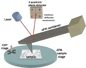
Vibrational analysis with scanning probe microscopy
The technique of vibrational analysis with scanning probe microscopy allows probing vibrational properties of materials at the submicrometer scale, and even of individual molecules.[1][2][3] This is accomplished by integrating scanning probe microscopy (SPM) and vibrational spectroscopy (Raman scattering or/and Fourier transform infrared spectroscopy, FTIR). This combination allows for much higher spatial resolution than can be achieved with conventional Raman/FTIR instrumentation. The technique is also nondestructive, requires non-extensive sample preparation, and provides more contrast such as intensity contrast, polarization contrast and wavelength contrast, as well as providing specific chemical information and topography images simultaneously.
History
Raman-NSOM
Near-field scanning optical microscopy (NSOM) was described in 1984,[4] and used in many applications since then.[5] The combination of Raman scattering and NSOM techniques was first realized in 1995, when it was used for imaging a Rb-doped KTP crystal at a spatial resolution of 250 nm.[6]
NSOM employs two different methods for data collection and analysis: the fiber tip aperture approach and the apertureless metal tip approach.[1] NSOM with aperture probes has a smaller aperture that can increase the spatial resolution of NSOM; however, the transmission of light to the sample and the collection efficiency of the scattered/emitted light is also diminished.[7] The apertureless near-field scanning microscopy (ANSOM) was developed in the 1990s. ANSOM employs a metalized tip instead of an optical fiber probe. The performance of the ANSOM strongly depends on the electric field enhancement factor of the metalized tip. This technique is based on surface plasmon resonance (SPR) which is the precursor of tip-enhanced Raman scattering (TERS) and surface-enhanced Raman scattering (SERS).
In 1997, Martin and Girard demonstrated theoretically that electric field under a metallic or dielectric tip (belonging to NSOM apertureless technique) can be strongly enhanced if the incident field is along the tip axis. Since then a few groups have reported Raman or fluorescence enhancement in near field optical spectroscopy by apertureless microscopy.[8] In 2000, T. Kalkbrenner et al. used a single gold particle as a probe for apertureless scanning and presented images of an aluminium film with 3 μm holes on a glass substrate.[9] The resolution of this apertureless method was 100 nm, that is comparable to that of fiber-based systems[9] Recently, a carbon nanotube (CNT) having a conical end, tagged with gold nanoparticles, was applied as a nanometer-resolution optical probe tip for NSOM.[10] NSOM images were obtained with a spatial resolution of ~5 nm, demonstrating the potential of a composite CNT probe tip for nanoscale-resolution optical imaging.
Tip-enhanced Raman scattering
There are two options for realizing apertureless NSOM-Raman technique: TERS and SERS. TERS is frequently used for apertureless NSOM-Raman and can significantly enhance the spatial resolution. This technique requires a metal tip to enhance the signal of the sample. That is why an AFM metal tip is usually used for enhancing the electric field for molecule excitation. Raman spectroscopy was combined with AFM in 1999.[11][12] A very narrow aperture of the tip was required to obtain a relatively high spatial resolution; such aperture reduced the signal and was difficult to prepare. In 2000, Stȍckle et al.[13] first designed a setup combining apertureless NSOM, Raman and AFM techniques, in which the tip had a 20 nm thick granular silver film on it. They reported a large gain in the Raman scattering intensity of a dye film (brilliant cresyl blue) deposited on a glass substrate if a metal-coated AFM tip was brought very close to the sample. About 2000-fold enhancement of Raman scattering and a spatial resolution of ~55 nm were achieved.[14]
Similarly, Nieman et al.[15] used an illuminated AFM tip coated with a 100 nm thick film of gold to enhance Raman scattering from polymers samples and achieved a resolution of 100 nm. In the early research of TERS, the most commonly used coating materials for the tip probe were silver and gold.[14][15] High-resolution spatial maps of Raman signals were obtained with this technique from molecular films of such compounds as brilliant cresyl blue, malachite green isothiocyanate and rhodamine 6G,[16] as well as individual carbon nanotubes.[17]
IR-NSOM and AFM
IR near-field scanning optical microscopy (IR-NSOM) is a powerful spectroscopic tool because it allows subwavelength resolution in IR spectroscopy. Previously, IR-NSOM was realized by applying a solid immersion lens with a refractive index of n, which shortens wavelength (λ) to (λ/n), compared to FTIR-based IR microscopy.[18] In 2004, an IR-SNOM achieved a spatial resolution ~λ/7 that is less than 1 μm.[18] This resolution was further improved to about λ/60 that is 50–150 nm for a boron nitride thin film sample.[19]
IR-NSOM uses an AFM to detect the absorption response of a material to the modulated infrared radiation from an FTIR spectrometer and therefore is also referred to as AFM/FTIR spectroscopy. Two approaches have been used to measure the response of polymer systems to infrared absorption. The first mode relies on the AFM contact mode, and the second mode of operation employs a scanning thermal microscopy probe (invented in 1986[20]) to measure the polymer's temperature increase. In 2007, AFM was combined with infrared attenuated total reflection (IR-ATR) spectroscopy to study the dissolution process of urea in a cyclohexane/butanol solution with a high spatial resolution.[21]
Theory and instrumentation
Raman-NSOM
There are two modes for the operation of NSOM technique,[5][22] with and without an aperture. These two mode have also been combined with the near-field Raman spectroscopy.[7][23][24] The near-field aperture must be nanosized that complicates the probe manufacturing process.[25] Also, the aperture method usually has a very weak signal due to weak excitation and Raman scattering signal. Overall, these factors lower the signal-to-noise ratio in aperature based NSOM/Raman technique. Apertureless probes are based on a metal-coated tip and provide a stronger signal.[26]
Aperture-based detection
Although the apertureless mode is more promising than the aperture mode, the latter is more widely used because of easier instrumental setup and operation. To obtain a high resolution Raman micrograph/spectrum, the following conditions should be met: (1) the size of the aperture must be on the order of the wavelength of the excitation light. (2) The distance from the tip of the probe to the sample must be smaller than excitation wavelength. (3) The instrument must remain stable over a long time. An important AFM feature is the ability to accurately control the distance between the sample and probe tip, which is the reason why the AFM-Raman combination is preferred for realizing Raman-NSOM.
Apertureless mode
The main drawback of the aperture mode is that the small aperture size reduces the signal intensity and is difficult to fabricate. Recently, researchers have focused on the apertureless mode, which utilizes SPR theory to produce stronger signals. There are two techniques supporting this mode: SERS and TERS.
TERS technique
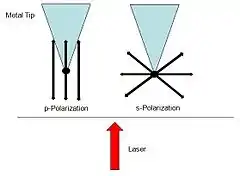
Theory and instrumentation of Raman/AFM and IR/AFM combine the theory of SPR (AFM and NSOM) and Raman scattering, and this combination is based on TERS. In TERS, the electric field of excitation source induces an SPR in the tip of the probe. If the electric field vector of the incidence light is perpendicular (s-polarized) to the metal tip axis, the free electrons are driven to the sides lateral of the tip. If it is parallel (p-polarized) to the tip axis, the free electrons on the surface of the metal are confined to the end of the apex of tip. As a consequence, there is a very large electric-field enhancement which is sensed by the molecules close to it leading to a stronger signal.[26]
A typical approach in a TERS experiment is to focus the laser beam on a metal tip with the light polarized along the tip axis, followed by collection of the surface-enhanced Raman scattered light from the sample in the enhancement zone of the tip using optics.[14]
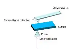
Depending on the sample and experiment, different illumination geometries have been applied in TERS experiments, as shown in figure 4. With p-polarized (parallel to the surface normal) incidence light, the plasmon excitation at the tip is most efficient. If the focusing objective lens is also used for collecting the scattered photons (backscattering geometry), the optimum angle is around 55° with respect to the surface normal. This is because the scattering lobe is maximum with this configuration and it provides a much enhanced signal.[27] The setup of figure 4(A) is usually used for the large thick samples. Setup (B) handles semi-transparent or transparent samples, such as single cells, tissue samples and biopolymers.[14] The setup of figure 4(C) is preferred for opaque samples because all the light would be focused by the parabolic mirror.
 |
 |
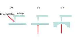 |
| Figure 2. S- and p-polarization with laser excitation.[28] | Figure 3. TERS setup using the back-excitation mode.[28] | Figure 4. TERS setup: (A) side illumination (p polarized); (B) in-line illumination (objective, s-polarized); (C) in-line illumination (parabolic mirror).[28] |
Comparison of TERS and SERS
Both TERS and SERS rely on a localized surface plasmon for increasing the ought-to-be weak Raman signal.[29] The only difference between them is that the sample in SERS has a rough surface that hinders application of a sharp AFM-like tip. TERS, on the other hand, uses a metal-coated tip having some roughness at nanoscale.[30][31] The “hot spot” theory[32] is very popular in explaining the large enhancement in the signal. That is, the signal from “hot spots” on the surface of the sample dominates the total signal from the sample.[33] This is also reinforced by the fact that the distance between nanoparticles and sample is an important factor in obtaining high Raman signal.
Raman/AFM instrumentation
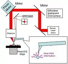
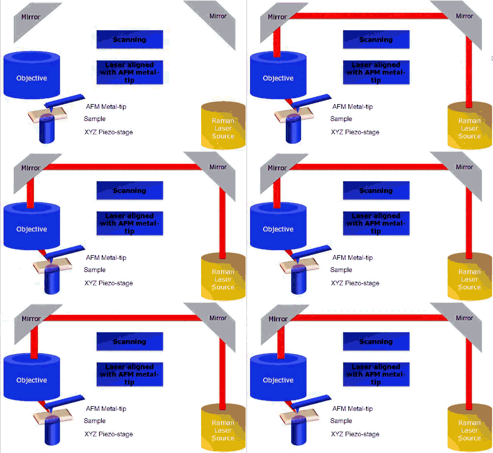
The Raman/AFM technique has two approaches: aperture and apertureless, and the apertureless mode is realized with SERS and TERS. Figure 5 is the example of an integrated TERS system. It shows that there are five main components for a whole integrated TERS (apertureless) system. These components are: microscope, one objective lens, one integrated AFM head, a Raman spectrometer and a CCD. The laser is focused on the sample, on piezo-stage and the AFM tip by the moving the laser beam along the tip. The movement of the laser beam is achieved by the mirror in the top left corner. The XYZ piezo-stage in the left bottom holds the sample. In this design, the laser beam is focused on the sample through an objective lens, and the scattered light is collected by the same lens.
This setup utilizes a low contact-pressure to reduce the damage to the AFM tip and sample.[21] The laser power is typically below 1 mW.[21] The notch filter can filter Rayleigh scattering from the excitation laser light from the back of the cantilever. The laser beam is focused on the apex of the gold-coated AFM tip and the sample. The laser scanning is completed by the moving the mirror across the approaching tip. A small enhance in background occurs when the laser spot focuses on the tip area. The movement of the XYZ piezo-stage finishes the sample scanning. The wide red signal is Raman signal which is collected through the objective lens. The same lens is also used for excitation of the sample and collecting the Raman signal.
NSOM/FTIR, AFM/FTIR and AFM-IR
Because of the diffraction limit in the resolution of conventional lens-based microscopes, namely D = 0.61λ/nsinθ,[34] the maximum resolution obtainable with an optical microscope is ~200 nm. A new type of lens using multiple scattering of light allowed to improve the resolution to about 100 nm.[35] Several new microscopy techniques with a sub-nanometer resolution have been developed in the last several decades, such as electron microscopy (SEM and TEM) and scanning probe microscopy (NSOM, STM and AFM). SPM differs from other techniques in that the excitation and signal collection are very close (less than diffraction limit distance) to the sample. Instead of using a conventional lens to obtain magnified images of samples, an SPM scans across the sample with a very sharp probe. Whereas SEM and TEM usually require vacuum and an extensive sample preparation, SPM measurements can be performed in atmospheric or liquid conditions.
Despite the achievable resolution of atomic scale for AFM and NSOM techniques, it does not provide chemical information of the sample. The infrared part of the electromagnetic spectrum covers molecular vibrations which can characterize chemical bonding within the sample.[36]
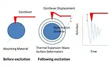
By combining SPM and vibrational spectroscopy, AFM/IR-NSOM and AFM-IR have emerged as useful characterization tools that integrate the high spatial resolution abilities of AFM with IR spectroscopy.[37][38][39][40][41][42][43][44][45] This new technique can be referred to as AFM/FTIR and NSOM/FTIR. AFM and NSOM can be used to detect the response when a modulated infrared radiation generated by an FTIR spectrometer is absorbed by a material. In the AFM-IR technique the absorption of the radiation by sample will cause a rapid thermal expansion wave which will be transferred to the vibrational modes of the AFM cantilever. Specifically, thermal expansion wave induces a vertical displacement of the ATM tip (Figure 6).[46] A local IR absorption spectrum then can be obtained through the measurement of the amplitude of the cantilever, which is a function of the IR source wavelength. For example, when the radiation laser wavelength is tuned at the resonance frequency with the vibrational absorption frequency of the sample, the displacement intensity of the cantilever will increase until the laser wavelength reaches the maximum of sample absorption.[46] The displacement of the cantilever will then be reduced as the laser wavelength is tuned past the absorption maximum. This approach can map chemical composition beyond the diffraction-limit resolution and can also provide three-dimensional topographic, thermal and mechanical information at the nanoscale. Overall, it overcomes the resolution limit of traditional IR spectroscopy and adds chemical and mechanical mapping to the AFM and NSOM.
Infrared light source
The ideal IR source should be monochromatic and tunable within a wide range of wavelength. According to T ∝d4/λ4, where T is the transmission coefficient, d the aperture diameter and λ is wavelength, the aperture-based NSOM/FTIR transmission is even more limited due to the long infrared wavelength;[47][48] therefore, an intense IR source is needed to offset the low transmission through the optical fiber. The common bright IR light sources are the free-electron laser (FEL),[2][39][45] color-center lasers, CO2 lasers and laser diodes. FEL is an excellent IR source, with 2–20 μm spectral range,[49][50] short pulses (picosecond) and high average power (0.1-1 W). Alternately, a tabletop picosecond optical parametric oscillator (OPO) can be used which is less expensive, but has a limited tunability and a lower power-output.[44][51]
NSOM/FTIR experimental setup
The essence of NSOM/FTIR is that it allows the detection of non-propagating evanescent waves in the near-field (less than one wavelength from the sample), thus yielding high spatial resolution. Depending on the detection modes of these non-propagating evanescent waves, two NSOM/FTIR instrumentations are available: apertureless NSOM/FTIR and aperture-based NSOM/FTIR.
- Aperture-based NSOM/FTIR
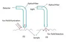
In aperture-based NSOM/FTIR, the probe is a waveguide with a tapered tip with a very small, sub-wavelength size aperture. When the aperture is brought into the near-field, it collects the non-propagating light and guides it to the detector. In general, there are two modes when the aperture is scanned over the sample: illumination mode and collection mode (Figure 7).
The high-quality infrared fiber tip is very important in realizing NSOM/FTIR technique. There are several types of fibers, such as sapphire, chalcogenide glass, fluoride glass and hollow silica guides.[52] Chalcogenide glasses are widely used because of their high transmittance in the broad IR range of 2–12 μm.[53] The fluoride fibers also exhibit low transmitting losses beyond 3.0 μm.
- Apertureless NSOM/FTIR
The probe is a sharp metal tip ending with a single or a few atoms. The sample is illuminated from far-field and the radiation is focused at the contact area between probe and sample. When this tip approaches the sample, usually within 10 nm, the incident electromagnetic field is enhanced due to the resonant surface plasma excitation as well as due to hot-spots in the sharp tip. The dipole interaction between the tip and sample change the non-propagating waves into propagating waves by scattering, and a detector collects the signal in the far-field. An apertureless NSOM/FTIR usually has better resolution (~5–30 nm) compared with aperture-based NSOM/FTIR (~50–150 nm). One main challenge in apertureless NSOM/FTIR is a strong background signal because the scattering is obtained from both near-field and remote area of the probe. Thus, the small near-field contribution to the signal has to be extracted from the background. One solution is to use a very flat sample with only optical spatial fluctuation.[54] Another solution is to apply constant-height mode scanning or pseudo-constant-height mode scanning.[55]
- Experimental scheme of aperture-based NSOM/FTIR
Figure 8 shows the experimental setup used in NSOM/FTIR in the external reflection mode. FEL source is focused on the sample from the far-field using a mirror. The distance between the probe and a sample is kept at a few nanometers during scanning.
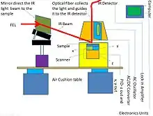
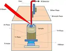
Figure 9 is the cross-section of a NSOM/FTIR instrument. As shown below, sample is placed on a piezo-electric tube scanner, in which the x-y tube has four parts, namely x+, x-, y+ and y-. Lateral (x-y plane) oscillation of the fiber tip is induced by applying an AC voltage to a dither piezo-scanner. Also, the fiber tip is fixed to a bimorph piezo-scanner so that the amplitude of the oscillation of the tip can be monitored through the scanner.
AFM/FTIR setup
- Spatial resolution
The spatial resolution of an AFM/FTIR instrument is related to the contact area between the probe and sample.[57] The contact area is given by a3 = 3PR/4E* and 1/E* = (1-n12)/ E1+ (1-n22)/ E2, where P is the force employed to the probe, n1 and n2 represent the Poisson ratios of the sample and probe, respectively, and E1 and E2 are the elastic moduli of the sample and probe materials respectively.[58] Typically, an AFM/FTIR has a resolution of 50–400 nm, for example, 100 nm,[43] λ/150,[40] and λ/400.[41]
- Instrumentation
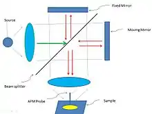
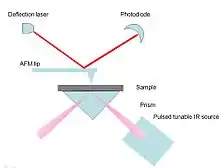
In AFM/FIIR, an AFM probe is used to measure the absorption response of the sample to infrared radiation. The general approach for AFM/FTIR is shown in Figure 10.[59]
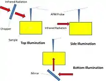
There are a few different experimental setups when the infrared radiation is projected onto the sample as shown below: top, side, and bottom illumination setups (Figure 11).[3]
Specifically, a sample is mounted onto an infrared-transparent zinc selenide prism for excitation purposes (Figure 12), then an optical parametric oscillator (OPO)-based tunable IR lased is radiated on the molecules to be probed by the instrument. Similar to conventional ATR spectroscopy, IR beam illuminates the sample through total internal reflection mechanism (Figure 12). The sample will heat up while absorbing radiation which causes a rapid thermal expansion of the sample surface.[40][44] This expansion will increase the resonant oscillations of the AFM cantilever in a characteristic ringdown pattern (ringdown patterns means the decay of cantilever oscillation exponential in nature[44]). Through Fourier transformation analysis, the signal could be isolated to obtain the amplitudes and frequencies of the oscillations. The amplitudes of the cantilever provide information of local absorption spectra, whereas the oscillation frequencies depend on the mechanical stiffness of the sample (Figure 12).[43][44]
Pros and cons
NSOM combined with FTIR/Raman technisues can provide local chemical information together with topographical details. This technique is non-destructive and can work in a variety of environments (liquids), for example, when detecting single biomolecules.[18][58][60][61] The illuminated area of sample is relatively big at around 1 μm. However, the sampling area is only ~10 nm. This means that a strong background from an unclean tip contributes to the overall signal, hindering the signal analysis.[55]
The Raman spectroscopy in general could be time-consuming due to the low scattering efficiency (<1 in 107 photons). It usually takes several minutes to accumulate a conventional Raman spectrum, and this time could be much longer in Raman-NSOM; for example, 9 hours for a 32×32-pixel image.[6][19] As to near-field IR/AFM, high optical losses in aqueous environments (water is strongly absorbing in the IR range) reduces the signal-to-noise ratio.[18][62]
Applications
Improving the resolution and enhancing the instrumentation with user-friendly hardware and software will make AFM/NSOM coupled with IR/Raman a useful characterization tool in many areas including biomedical, materials and life sciences.[63] For example, this technique was used in detecting the spin-cast thin film of poly(dimethylsiloxane) with polystyrene on it by scanning the tip over the sample. The shape and size of polystyrene fragments was detected at a high spatial resolution due to its high absorption at specific resonance frequencies.[64] Other examples include inorganic boron nitride thin films characterization with IR-NSOM.[16] The images of single molecule rhodamine 6G (Rh-6G) was obtained with a spatial resolution of 50 nm.[65] These techniques can be also used in numerous biological related applications including the analysis of plant materials, bone, and single cells. Biological application was demonstrated by detecting details of conformation changes of cholesteryl-oleate caused by FEL irradiation with a spatial resolution below the diffraction limit.[66] Researchers also used Raman/NSOM in tracking the formation of energy-storing polymer polyhydroxybutyrate in bacteria Rhodobacter capsulatus.[67]
This characterization tool may also help in the kinetic studies on physical and chemical processes at a wide variety of surfaces giving chemical specificity via IR spectroscopy as well as high-resolution imaging via AFM.[18] For example, the study of the hydrogen termination of Si (100) surface was performed by studying the absorbance of Si-O bond to characterize the reaction between silicon surface and atmospheric oxygen.[68] Studies were also conducted where the reactivity of a polymer, a 1000-nm-thick poly-(tert-butylmethacrylate) (PTBMA) combined with a photochemically modified 500-nm-thick poly(methacrylic acid) (PMAA), with water vapor depicted the different absorption bands before and after water uptake by the polymer. Not only the increased swell of PMAA (280 nm) was observed but also the different absorption ability of water was shown by the different transmission of IR light at a much smaller dimension (<500 nm). These results are related to polymer, chemical and biological sensors, and tissue engineering and artificial organ studies.[69] Because of their high spatial resolution, NSOM/AFM-Raman/IR techniques can be used for measuring the width of multilayer films, including layers which are too small (in the x and y directions) to be probed with conventional IR or Raman spectroscopy.[39]
References
- Dragnea, Bogdan; Leone, Stephen (2001). "Advances in submicron infrared vibrational band chemical imaging". International Reviews in Physical Chemistry. 20 (1): 59–92. Bibcode:2001IRPC...20...59D. doi:10.1080/01442350010012557. S2CID 9166775.
- Vobornik, Dušan (2005). "Scanning near-field infrared microscopy and spectromicroscopy applied to nano-systems and cells". doi:10.5075/epfl-thesis-3296. Retrieved 15 July 2013. Cite journal requires
|journal=(help) - Boerio, F. J.; Starr, M. J. (2008). "AFM/FTIR: A New Technique for Materials Characterization". The Journal of Adhesion. 84 (10): 872–895. doi:10.1080/00218460802445308. S2CID 85439894.
- Oshikane, Yasushi; Kataoka, Toshihiko; Okuda, Mitsuru; Hara, Seiji; Inoue, Haruyuki; Nakano, Motohiro (2007). "Observation of nanostructure by scanning near-field optical microscope with small sphere probe". Science and Technology of Advanced Materials. 8 (3): 181–185. Bibcode:2007STAdM...8..181O. doi:10.1016/j.stam.2007.02.013. S2CID 3891418.
- Webster, S (1998). "Raman microscopy using a scanning near-field optical probe". Vibrational Spectroscopy. 18: 51–59. doi:10.1016/S0924-2031(98)00037-X.
- Jahncke, C. L.; Paesler, M. A.; Hallen, H. D. (1995). "Raman imaging with near-field scanning optical microscopy". Applied Physics Letters. 67 (17): 2483. Bibcode:1995ApPhL..67.2483J. doi:10.1063/1.114615. S2CID 34846438.
- Pettinger, Bruno (2010). "Single-molecule surface- and tip-enhanced Raman spectroscopy". Molecular Physics. 108 (16): 2039–2059. Bibcode:2010MolPh.108.2039P. doi:10.1080/00268976.2010.506891. S2CID 220376286.
- J. J. Wang; et al. (2003). "Apertureless near-field Raman spectroscopy". Journal of Microscopy. 210 (3): 330–333. doi:10.1046/j.1365-2818.2003.01166.x. PMID 12787109.
- Kalkbrenner, T.; Ramstein, M.; Mlynek, J.; Sandoghdar, V. (2001). "A single gold particle as a probe for apertureless scanning near-field optical microscopy". Journal of Microscopy. 202 (Pt 1): 72–76. doi:10.1046/j.1365-2818.2001.00817.x. PMID 11298873. S2CID 33056571.
- Nakata, Toshihiko; Watanabe, Masahiro (2011). "Nanometer-resolution optical probe using a metallic-nanoparticle-intercalated carbon nanotube". Journal of Applied Physics. 109 (1): 013110–013110–5. Bibcode:2011JAP...109a3110N. doi:10.1063/1.3511437.
- Inouye, Yasushi (1999). "Near-field scanning optical microscope using a metallized cantilever tip for nanospectroscopy". 3791: 40–48. doi:10.1117/12.363860. S2CID 136975757. Cite journal requires
|journal=(help) - Anderson, Mark S.; Pike, William T. (2002). "A Raman-atomic force microscope for apertureless-near-field spectroscopy and optical trapping". Review of Scientific Instruments. 73 (3): 1198. Bibcode:2002RScI...73.1198A. doi:10.1063/1.1445864.
- Stöckle, R (2000). "Nanoscale chemical analysis by tip-enhanced Raman spectroscopy". Chemical Physics Letters. 318 (1–3): 131–136. Bibcode:2000CPL...318..131S. doi:10.1016/S0009-2614(99)01451-7.
- Bruno Pettinger, Tip-Enhanced Raman Spectroscopy (TERS)
- Nieman, Linda T.; Krampert, Gerhard M.; Martinez, Robert E. (2001). "An apertureless near-field scanning optical microscope and its application to surface-enhanced Raman spectroscopy and multiphoton fluorescence imaging". Review of Scientific Instruments. 72 (3): 1691. Bibcode:2001RScI...72.1691N. doi:10.1063/1.1347975.
- Elfick, Alistair P. D.; Downes, Andrew R.; Mouras, Rabah (2009). "Development of tip-enhanced optical spectroscopy for biological applications: A review". Analytical and Bioanalytical Chemistry. 396 (1): 45–52. doi:10.1007/s00216-009-3223-9. PMID 19876621. S2CID 44849038.
- Chan, K L Andrew; Kazarian, Sergei G (2011). "Tip-enhanced Raman mapping with top-illumination AFM". Nanotechnology. 22 (17): 175701. Bibcode:2011Nanot..22q5701C. doi:10.1088/0957-4484/22/17/175701. PMID 21411920. S2CID 26859123.
- Masaki, Tatsuhiro; Inouye, Yasushi; Kawata, Satoshi (2004). "Submicron resolution infrared microscopy by use of a near-field scanning optical microscope with an apertured cantilever". Review of Scientific Instruments. 75 (10): 3284–3287. Bibcode:2004RScI...75.3284M. doi:10.1063/1.1784567.
- Vobornik, D; Margaritondo, G; Sanghera, J; Thielen, P; Aggarwal, I; Ivanov, B; Tolk, N; Manni, V; et al. (2005). "Spectroscopic infrared scanning near-field optical microscopy (IR-SNOM)". Journal of Alloys and Compounds. 401 (1–2): 80–85. doi:10.1016/j.jallcom.2005.02.057.
- Williams, C. C.; Wickramasinghe, H. K. (1986). "Scanning thermal profiler". Applied Physics Letters. 49 (23): 1587. Bibcode:1986ApPhL..49.1587W. doi:10.1063/1.97288.
- Brucherseifer, Martin; Kranz, Christine; Mizaikoff, Boris (2007). "Combined in Situ Atomic Force Microscopy- Infrared-Attenuated Total Reflection Spectroscopy". Analytical Chemistry. 79 (22): 8803–8806. doi:10.1021/ac071004q. PMID 17939644.
- Hecht, Bert; Sick, Beate; Wild, Urs P.; Deckert, Volker; Zenobi, Renato; Martin, Olivier J. F.; Pohl, Dieter W. (2000). "Scanning near-field optical microscopy with aperture probes: Fundamentals and applications". The Journal of Chemical Physics. 112 (18): 7761. Bibcode:2000JChPh.112.7761H. doi:10.1063/1.481382.
- Sands, H. S.; Demangeot, F.; Bonera, E.; Webster, S.; Bennett, R.; Hayward, I. P.; Marchi, F.; Smith, D. A.; et al. (2002). "Development of a combined confocal and scanning near-field Raman microscope for deep UV laser excitation". Journal of Raman Spectroscopy. 33 (9): 730–739. Bibcode:2002JRSp...33..730S. doi:10.1002/jrs.909.
- Verma, Prabhat; Yamada, Kohei; Watanabe, Hiroyuki; Inouye, Yasushi; Kawata, Satoshi (2006). "Near-field Raman scattering investigation of tip effects on C60 molecules". Physical Review B. 73 (4): 045416. Bibcode:2006PhRvB..73d5416V. doi:10.1103/PhysRevB.73.045416.
- Novotny, L.; Pohl, D. W.; Hecht, B. (1995). "Scanning near-field optical probe with ultrasmall spot size". Optics Letters. 20 (9): 970. Bibcode:1995OptL...20..970N. doi:10.1364/OL.20.000970. PMID 19859393.
- Qian, X.-M.; Nie, S. M. (2008). "Single-molecule and single-nanoparticle SERS: From fundamental mechanisms to biomedical applications". Chemical Society Reviews. 37 (5): 912–20. doi:10.1039/B708839F. PMID 18443676.
- Rendell, R.; Scalapino, D. (1981). "Surface plasmons confined by microstructures on tunnel junctions". Physical Review B. 24 (6): 3276–3294. Bibcode:1981PhRvB..24.3276R. doi:10.1103/PhysRevB.24.3276.
- AFM-microRaman and nanoRamanTM
- [What TERS microscopy can do, SERS cannot What TERS microscopy can do, SERS cannot] Satoshi Kawata Department of Applied Physics, Osaka University, Suita, Osaka and RIKEN, Wako, Saitama, Japan
- Kawata, Satoshi; Inouye, Yasushi; Verma, Prabhat (2009). "Plasmonics for near-field nano-imaging and superlensing". Nature Photonics. 3 (7): 388–394. Bibcode:2009NaPho...3..388K. doi:10.1038/nphoton.2009.111.
- Yano, Taka-aki; Verma, Prabhat; Saito, Yuika; Ichimura, Taro; Kawata, Satoshi (2009). "Pressure-assisted tip-enhanced Raman imaging at a resolution of a few nanometres". Nature Photonics. 3 (8): 473–477. Bibcode:2009NaPho...3..473Y. doi:10.1038/nphoton.2009.74. S2CID 54837097.
- Ichimura, Taro; Hayazawa, Norihiko; Hashimoto, Mamoru; Inouye, Yasushi; Kawata, Satoshi (2004). "Tip-Enhanced Coherent Anti-Stokes Raman Scattering for Vibrational Nanoimaging". Physical Review Letters. 92 (22): 220801. Bibcode:2004PhRvL..92v0801I. doi:10.1103/PhysRevLett.92.220801. PMID 15245207. S2CID 29726570.
- Pettinger B.Topics Appl. Phys., 103, 217–240 (2006)
- L. Rayleigh, Phil. Mag.. 8, 261–274 (1879)
- E.G. van Putten; D. Akbulut; J. Bertolotti; W.L. Vos; A. Lagendijk & A.P. Mosk (2011). "Scattering Lens Resolves Sub-100 nm Structures with Visible Light". Physical Review Letters. 106 (19): 193905. arXiv:1103.3643. Bibcode:2011PhRvL.106s3905V. doi:10.1103/PhysRevLett.106.193905. PMID 21668161. S2CID 15793849.
- R. M. Silverstein, G. C. Bassler, T. C. Morill, Spectrometric Identification of Organic Compounds, 5th edition, Wiley, New York (1991) ISBN 0-471-39362-2
- Hammiche, A.; Pollock, H. M.; Reading, M.; Claybourn, M.; Turner, P. H.; Jewkes, K. (1999). "Photothermal FT-IR Spectroscopy: A Step Towards FT-IR Microscopy at a Resolution Better Than the Diffraction Limit". Applied Spectroscopy. 53 (7): 810–815. Bibcode:1999ApSpe..53..810H. doi:10.1366/0003702991947379. S2CID 93359289.
- Hammiche, A.; Bozec, L.; Conroy, M.; Pollock, H. M.; Mills, G.; Weaver, J. M. R.; Price, D. M.; Reading, M.; et al. (2000). "Highly localized thermal, mechanical, and spectroscopic characterization of polymers using miniaturized thermal probes". Journal of Vacuum Science and Technology B. 18 (3): 1322. Bibcode:2000JVSTB..18.1322H. doi:10.1116/1.591381. S2CID 55856483.
- Brehm, Markus; Taubner, Thomas; Hillenbrand, Rainer; Keilmann, Fritz (2006). "Infrared Spectroscopic Mapping of Single Nanoparticles and Viruses at Nanoscale Resolution". Nano Letters. 6 (7): 1307–1310. Bibcode:2006NanoL...6.1307B. doi:10.1021/nl0610836. PMID 16834401.
- Julien Houel; et al. (2007). "Ultraweak-Absorption Microscopy of a Single Semiconductor Quantum Dot in the Midinfrared Range". Physical Review Letters. 99 (21): 217404. Bibcode:2007PhRvL..99u7404H. doi:10.1103/PhysRevLett.99.217404. PMID 18233255. S2CID 13225150.
- Houel, Julien; Homeyer, Estelle; Sauvage, SéBastien; Boucaud, Philippe; Dazzi, Alexandre; Prazeres, Rui; Ortéga, Jean-Michel (2009). "Midinfrared absorption measured at a λ/400 resolution with an atomic force microscope". Optics Express. 17 (13): 10887–94. Bibcode:2009OExpr..1710887H. doi:10.1364/OE.17.010887. PMID 19550489. S2CID 120639500.
- Verity, Jocelyne E.; Chhabra, Neetu; Sinnathamby, Koneswaran; Yip, Christopher M. (2009). "Tracking Molecular Interactions in Membranes by Simultaneous ATR-FTIR-AFM". Biophysical Journal. 97 (4): 1225–1231. Bibcode:2009BpJ....97.1225V. doi:10.1016/j.bpj.2009.06.013. PMC 2726332. PMID 19686671.
- Kjoller, K; Felts, J R; Cook, D; Prater, C B; King, W P (2010). "High-sensitivity nanometer-scale infrared spectroscopy using a contact mode microcantilever with an internal resonator paddle". Nanotechnology. 21 (18): 185705. Bibcode:2010Nanot..21r5705K. doi:10.1088/0957-4484/21/18/185705. PMID 20388971.
- Craig Prater, Kevin Kjoller, Debra Cook, Roshan Shetty, Gregory Meyers, Carl Reinhardt, Jonathan Felts, William King, Konstantin Vodopyanov and Alexandre Dazzi, Nanoscale Infrared Spectroscopy of Materials by Atomic Force Microscopy Microscopy and Analysis, 24, 5–8 (2010)
- Yarrow, Fiona; Kennedy, Eamonn; Salaun, Frederic; Rice, James H. (2010). "Sub-wavelength infrared imaging of lipids". Biomedical Optics Express. 2 (1): 37–43. doi:10.1364/BOE.2.000037. PMC 3028496. PMID 21326633.
- Rice, James H. (2010). "Nanoscale optical imaging by atomic force infrared microscopy" (PDF). Nanoscale. 2 (5): 660–7. Bibcode:2010Nanos...2..660R. doi:10.1039/b9nr00279k. hdl:10197/4463. PMID 20648306.
- Bethe, H. (1944). "Theory of Diffraction by Small Holes". Physical Review. 66 (7–8): 163–182. Bibcode:1944PhRv...66..163B. doi:10.1103/PhysRev.66.163.
- C. J. Bouwkamp, Philips Res. Rep., 5, 321–332 (1950)
- Cricenti, A.; Generosi, R.; Perfetti, P.; Gilligan, J. M.; Tolk, N. H.; Coluzza, C.; Margaritondo, G. (1998). "Free-electron-laser near-field nanospectroscopy". Applied Physics Letters. 73 (2): 151. Bibcode:1998ApPhL..73..151C. doi:10.1063/1.121739.
- Glotin, F (1998). "Activities of the CLIO infrared facility". Nuclear Instruments and Methods in Physics Research Section B: Beam Interactions with Materials and Atoms. 144 (1–4): 8–17. Bibcode:1998NIMPB.144....8G. doi:10.1016/S0168-583X(98)00293-6.
- Tanimura, Takahito; Akamatsu, Daisuke; Yokoi, Yoshihiko; Furusawa, Akira; Kozuma, Mikio (2006). "Generation of a squeezed vacuum resonant on a rubidium D1 line with periodically poled KTiOPO4". Optics Letters. 31 (15): 2344–6. arXiv:quant-ph/0603214. Bibcode:2006OptL...31.2344T. doi:10.1364/OL.31.002344. PMID 16832480. S2CID 18700111.
- Sanghera, J. S., and Aggarwal, I. D., Infrared Fiber Optics (Boca Raton; Florida: CRC) 1998
- Mossadegh, R.; Sanghera, J.S.; Schaafsma, D.; Cole, B.J.; Nguyen, V.Q.; Miklos, R.E.; Aggarwal, I.D. (1998). "Fabrication of single-mode chalcogenide optical fiber". Journal of Lightwave Technology. 16 (2): 214–217. Bibcode:1998JLwT...16..214M. doi:10.1109/50.661012.
- Lahrech, A.; Bachelot, R.; Gleyzes, P.; Boccara, A. C. (1997). "Infrared near-field imaging of implanted semiconductors: Evidence of a pure dielectric contrast". Applied Physics Letters. 71 (5): 575. Bibcode:1997ApPhL..71..575L. doi:10.1063/1.119798. S2CID 11004387.
- Jordan, Claire E.; Stranick, Stephan J.; Richter, Lee J.; Cavanagh, Richard R. (1999). "Removing optical artifacts in near-field scanning optical microscopy by using a three-dimensional scanning mode". Journal of Applied Physics. 86 (5): 2785. Bibcode:1999JAP....86.2785J. doi:10.1063/1.371126.
- Cricenti, A.; Generosi, R.; Barchesi, C.; Luce, M.; Rinaldi, M. (1998). "A multipurpose scanning near-field optical microscope: Reflectivity and photocurrent on semiconductor and biological samples". Review of Scientific Instruments. 69 (9): 3240. Bibcode:1998RScI...69.3240C. doi:10.1063/1.1149089.
- Pethica, J B; Oliver, W C (1987). "Tip Surface Interactions in STM and AFM". Physica Scripta. T19A: 61–66. Bibcode:1987PhST...19...61P. doi:10.1088/0031-8949/1987/T19A/010.
- Palmer, R; Dittmar, R (1993). "Step-scan FT-IR photothermal spectral depth profiling of polymer films". Thin Solid Films. 223 (1): 31–38. Bibcode:1993TSF...223...31P. doi:10.1016/0040-6090(93)90724-4.
- Anderson, Mark S. (2000). "Infrared Spectroscopy with an Atomic Force Microscope". Applied Spectroscopy. 54 (3): 349–352. Bibcode:2000ApSpe..54..349A. doi:10.1366/0003702001949618. S2CID 95187852.
- Sun, W. X.; Shen, Z. X. (2003). "Near-field scanning Raman microscopy using apertureless probes". Journal of Raman Spectroscopy. 34 (9): 668–676. Bibcode:2003JRSp...34..668S. doi:10.1002/jrs.1063.
- Grausem, J.; Humbert, B.; Burneau, A.; Oswalt, J. (1997). "Subwavelength Raman spectroscopy". Applied Physics Letters. 70 (13): 1671. Bibcode:1997ApPhL..70.1671G. doi:10.1063/1.118665.
- Dragnea, Bogdan; Preusser, Jan; Schade, Wolfgang; Leone, Stephen R.; Hinsberg, William D. (1999). "Transmission near-field scanning microscope for infrared chemical imaging". Journal of Applied Physics. 86 (5): 2795. Bibcode:1999JAP....86.2795D. doi:10.1063/1.371127. S2CID 12908935.
- Webster, S.; Batchelder, D. N.; Smith, D. A. (1998). "Submicron resolution measurement of stress in silicon by near-field Raman spectroscopy". Applied Physics Letters. 72 (12): 1478. Bibcode:1998ApPhL..72.1478W. doi:10.1063/1.120598.
- Akhremitchev, Boris B.; Pollack, Steven; Walker, Gilbert C. (2001). "Apertureless Scanning Near-Field Infrared Microscopy of a Rough Polymeric Surface". Langmuir. 17 (9): 2774–2781. doi:10.1021/la001401v.
- Hayazawa, N (2000). "Metallized tip amplification of near-field Raman scattering". Optics Communications. 183 (1–4): 333–336. Bibcode:2000OptCo.183..333H. doi:10.1016/S0030-4018(00)00894-4.
- Masaki, Tatsuhiro (2004). "Near-field infrared imaging of molecular changes in cholesteryl oleate by free electron laser infrared ablation". Journal of Applied Physics. 95 (1): 334–338. Bibcode:2004JAP....95..334M. doi:10.1063/1.1628380.
- Mayet, Celine; Dazzi, Alexandre; Prazeres, Rui; Ortega, Jean-Michel; Jaillard, Danielle (2010). "In situ identification and imaging of bacterial polymer nanogranules by infrared nanospectroscopy". The Analyst. 135 (10): 2540–5. Bibcode:2010Ana...135.2540M. doi:10.1039/C0AN00290A. PMID 20820491.
- E. Romano, S. Trabattoni, M. Campione, E. Merati, A. Sassella and D. Narducci Combined use of AFM and FTIR in the analysis of the hydrogen termination of Si(100) surfaces Microscopy: Science, Technology, Applications and Education, A. Méndez-Vilas and J. Diaz (Eds.), Vol. 3, pp. 1984–1992 (2010) ISBN 978-84-614-6191-2
- McDonough, Laurie A.; Dragnea, Bogdan; Preusser, Jan; Leone, Stephen R.; Hinsberg, William D. (2003). "Water Vapor Uptake in Photolithographic Polymers Observed by Infrared Near-Field Scanning Optical Microscopy in a Controlled Environment". The Journal of Physical Chemistry B. 107 (21): 4951–4954. doi:10.1021/jp022489j. S2CID 18265192.
