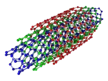
Carbon nanotube
Carbon nanotubes (CNTs) are tubes made of carbon with diameters typically measured in nanometers.
| Part of a series of articles on |
| Nanomaterials |
|---|
 |
| Carbon nanotubes |
| Fullerenes |
| Other nanoparticles |
| Nanostructured materials |
|
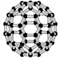
Carbon nanotubes often refer to single-wall carbon nanotubes (SWCNTs) with diameters in the range of a nanometer. They were discovered independently in 1993 by Iijima and Ichihashi [1] and Bethune et al.[2] in carbon arc chambers similar to those used to produce fullerenes. Single-wall carbon nanotubes are one of the allotropes of carbon, intermediate between fullerene cages and flat graphene.
Although not made this way, single-wall carbon nanotubes can be idealized as cutouts from a two-dimensional hexagonal lattice of carbon atoms rolled up along one of the Bravais lattice vectors of the hexagonal lattice to form a hollow cylinder. In this construction, periodic boundary conditions are imposed over the length of this roll up vector to yield a helical lattice of seamlessly bonded carbon atoms on the cylinder surface.[3]
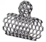
Carbon nanotubes also often refer to multi-wall carbon nanotubes (MWCNTs) consisting of nested single-wall carbon nanotubes[3] weakly bound together by van der Waals interactions in a tree ring-like structure. If not identical, these tubes are very similar to Oberlin, Endo and Koyama's long straight and parallel carbon layers cylindrically arranged around a hollow tube.[4] Multi-wall carbon nanotubes are also sometimes used to refer to double- and triple-wall carbon nanotubes.
Carbon nanotubes can also refer to tubes with an undetermined carbon-wall structure and diameters less than 100 nanometers. Such tubes were discovered in 1952 by Radushkevich and Lukyanovich.[5] [6]
While nanotubes of other compositions exist, most research has been focused on the carbon ones. Therefore, the "carbon" qualifier is often left implicit in the acronyms, and the names are abbreviated NT, SWNT, and MWNT.
The length of a carbon nanotube produced by common production methods is often not reported, but is typically much larger than its diameter. Thus, for many purposes end effects are neglected and the length of carbon nanotubes is assumed infinite.
Carbon nanotubes can exhibit remarkable electrical conductivity,[7] [8] while others are semiconductors.[9] [10] They also have exceptional tensile strength [11] and thermal conductivity,[12] [13] because of their nanostructure and strength of the bonds between carbon atoms. In addition, they can be chemically modified.[14] These properties are expected to be valuable in many areas of technology, such as electronics, optics, composite materials (replacing or complementing carbon fibers), nanotechnology, and other applications of materials science.
Rolling up a hexagonal lattice along different directions to form different infinitely long single-wall carbon nanotubes shows that all of these tubes not only have helical but also translational symmetry along the tube axis and many also have nontrivial rotational symmetry about this axis. In addition, most are chiral, meaning the tube and its mirror image cannot be superimposed. This construction also allows single-wall carbon nanotubes to be labeled by a pair of integers.[9]
A special group of achiral single-wall carbon nanotubes are metallic,[7] but all the rest are either small or moderate band gap semiconductors.[9] These electrical properties, however, do not depend on whether the hexagonal lattice is rolled from its back to front or from its front to back and hence are the same for the tube and its mirror image.[9]
Structure of single-walled tubes
The structure of an ideal (infinitely long) single-walled carbon nanotube is that of a regular hexagonal lattice drawn on an infinite cylindrical surface, whose vertices are the positions of the carbon atoms. Since the length of the carbon-carbon bonds is fairly fixed, there are constraints on the diameter of the cylinder and the arrangement of the atoms on it.[15]
The zigzag and armchair configurations
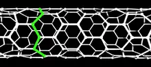
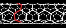
In the study of nanotubes, one defines a zigzag path on a graphene-like lattice as a path that turns 60 degrees, alternating left and right, after stepping through each bond. It is also conventional to define an armchair path as one that makes two left turns of 60 degrees followed by two right turns every four steps.
On some carbon nanotubes, there is a closed zigzag path that goes around the tube. One says that the tube is of the zigzag type or configuration, or simply is a zigzag nanotube. If the tube is instead encircled by a closed armchair path, it is said to be of the armchair type, or an armchair nanotube.
 Zigzag nanotube |
 Armchair nanotube |
An infinite nanotube that is of the zigzag (or armchair) type consists entirely of closed zigzag (or armchair) paths, connected to each other.
The (n,m) notation
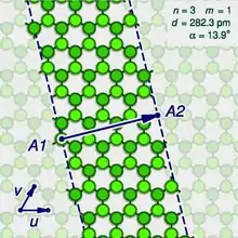
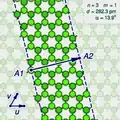
The zigzag and armchair configurations are not the only structures that a single-walled nanotube can have. To describe the structure of a general infinitely long tube, one should imagine it being sliced open by a cut parallel to its axis, that goes through some atom A, and then unrolled flat on the plane, so that its atoms and bonds coincide with those of an imaginary graphene sheet—more precisely, with an infinitely long strip of that sheet.
The two halves of the atom A will end up on opposite edges of the strip, over two atoms A1 and A2 of the graphene. The line from A1 to A2 will correspond to the circumference of the cylinder that went through the atom A, and will be perpendicular to the edges of the strip.
In the graphene lattice, the atoms can be split into two classes, depending on the directions of their three bonds. Half the atoms have their three bonds directed the same way, and half have their three bonds rotated 180 degrees relative to the first half. The atoms A1 and A2, which correspond to the same atom A on the cylinder, must be in the same class.
It follows that the circumference of the tube and the angle of the strip are not arbitrary, because they are constrained to the lengths and directions of the lines that connect pairs of graphene atoms in the same class.
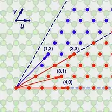
Let u and v be two linearly independent vectors that connect the graphene atom A1 to two of its nearest atoms with the same bond directions. That is, if one numbers consecutive carbons around a graphene cell with C1 to C6, then u can be the vector from C1 to C3, and v be the vector from C1 to C5. Then, for any other atom A2 with same class as A1, the vector from A1 to A2 can be written as a linear combination n u + m v, where n and m are integers. And, conversely, each pair of integers (n,m) defines a possible position for A2.[15]
Given n and m, one can reverse this theoretical operation by drawing the vector w on the graphene lattice, cutting a strip of the latter along lines perpendicular to w through its endpoints A1 and A2, and rolling the strip into a cylinder so as to bring those two points together. If this construction is applied to a pair (k,0), the result is a zigzag nanotube, with closed zigzag paths of 2k atoms. If it is applied to a pair (k,k), one obtains an armchair tube, with closed armchair paths of 4k atoms.
Nanotube types
Moreover, the structure of the nanotube is not changed if the strip is rotated by 60 degrees clockwise around A1 before applying the hypothetical reconstruction above. Such a rotation changes the corresponding pair (n,m) to the pair (−2m,n+m).
It follows that many possible positions of A2 relative to A1 — that is, many pairs (n,m) — correspond to the same arrangement of atoms on the nanotube. That is the case, for example, of the six pairs (1,2), (−2,3), (−3,1), (−1,−2), (2,−3), and (3,−1). In particular, the pairs (k,0) and (0,k) describe the same nanotube geometry.
These redundancies can be avoided by considering only pairs (n,m) such that n > 0 and m ≥ 0; that is, where the direction of the vector w lies between those of u (inclusive) and v (exclusive). It can be verified that every nanotube has exactly one pair (n,m) that satisfies those conditions, which is called the tube's type. Conversely, for every type there is a hypothetical nanotube. In fact, two nanotubes have the same type if and only if one can be conceptually rotated and translated so as to match the other exactly.
Instead of the type (n,m), the structure of a carbon nanotube can be specified by giving the length of the vector w (that is, the circumference of the nanotube), and the angle α between the directions of u and w, which may range from 0 (inclusive) to 60 degrees clockwise (exclusive). If the diagram is drawn with u horizontal, the latter is the tilt of the strip away from the vertical.
Here are some unrolled nanotube diagrams:
 Chiral nanotube of the (3,1) type.
 Chiral nanotube of the (1,3) type, mirror image of the (3,1) type.
 Nanotube of the (2,2) type, the narrowest "armchair" one
 Nanotube of the (3,0) type, the narrowest "zigzag" one
Chirality and mirror symmetry
A nanotube is chiral if it has type (n,m), with m > 0 and m ≠ n; then its enantiomer (mirror image) has type (m,n), which is different from (n,m). This operation corresponds to mirroring the unrolled strip about the line L through A1 that makes an angle of 30 degrees clockwise from the direction of the u vector (that is, with the direction of the vector u+v). The only types of nanotubes that are achiral are the (k,0) "zigzag" tubes and the (k,k) "armchair" tubes.
If two enantiomers are to be considered the same structure, then one may consider only types (n,m) with 0 ≤ m ≤ n and n > 0. Then the angle α between u and w, which may range from 0 to 30 degrees (inclusive both), is called the "chiral angle" of the nanotube.
Circumference and diameter
From n and m one can also compute the circumference c, which is the length of the vector w, which turns out to be

in picometres. The diameter of the tube is then , that is


also in picometres. (These formulas are only approximate, especially for small n and m where the bonds are strained; and they do not take into account the thickness of the wall.)
The tilt angle α between u and w and the circumference c are related to the type indices n and m by

where arg(x,y) is the clockwise angle between the X-axis and the vector (x,y); a function that is available in many programming languages as atan2(y,x). Conversely, given c and α, one can get the type (n,m) by the formulas

which must evaluate to integers.
Physical limits
Narrowest nanotubes
If n and m are too small, the structure described by the pair (n,m) will describe a molecule that cannot be reasonably called a "tube", and may not even be stable. For example, the structure theoretically described by the pair (1,0) (the limiting "zigzag" type) would be just a chain of carbons. That is a real molecule, the carbyne; which has some characteristics of nanotubes (such as orbital hybridization, high tensile strength, etc.) — but has no hollow space, and may not be obtainable as a condensed phase. The pair (2,0) would theoretically yield a chain of fused 4-cycles; and (1,1), the limiting "armchair" structure, would yield a chain of bi-connected 4-rings. These structures may not be realizable.
The thinnest carbon nanotube proper is the armchair structure with type (2,2), which has a diameter of 0.3 nm. This nanotube was grown inside a multi-walled carbon nanotube. Assigning of the carbon nanotube type was done by a combination of high-resolution transmission electron microscopy (HRTEM), Raman spectroscopy, and density functional theory (DFT) calculations.[16]
The thinnest freestanding single-walled carbon nanotube is about 0.43 nm in diameter.[17] Researchers suggested that it can be either (5,1) or (4,2) SWCNT, but the exact type of the carbon nanotube remains questionable.[18] (3,3), (4,3), and (5,1) carbon nanotubes (all about 0.4 nm in diameter) were unambiguously identified using aberration-corrected high-resolution transmission electron microscopy inside double-walled CNTs.[19]
Here are some tube types that are "degenerate" for being too narrow:
 Degenerate "zigzag" tube type (1,0)
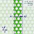 Degenerate "zigzag" tube type (2,0)
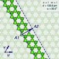 Degenerate "armchair" tube type (1,1)
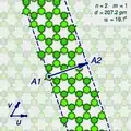 Possibly degenerate chiral tube type (2,1)
Length
The observation of the longest carbon nanotubes grown so far, around 1/2 meter (550 mm long), was reported in 2013.[20] These nanotubes were grown on silicon substrates using an improved chemical vapor deposition (CVD) method and represent electrically uniform arrays of single-walled carbon nanotubes.[21]
The shortest carbon nanotube can be considered to be the organic compound cycloparaphenylene, which was synthesized in 2008 by Ramesh Jasti.[22] Other small molecule carbon nanotubes have been synthesized since.[23]
Density
The highest density of CNTs was achieved in 2013, grown on a conductive titanium-coated copper surface that was coated with co-catalysts cobalt and molybdenum at lower than typical temperatures of 450 °C. The tubes averaged a height of 380 nm and a mass density of 1.6 g cm−3. The material showed ohmic conductivity (lowest resistance ∼22 kΩ).[24][25]
Variants
There is no consensus on some terms describing carbon nanotubes in scientific literature: both "-wall" and "-walled" are being used in combination with "single", "double", "triple", or "multi", and the letter C is often omitted in the abbreviation, for example, multi-walled carbon nanotube (MWNT). International Standards Organization uses single-wall or multi-wall in its documents.
Multi-walled
Multi-walled nanotubes (MWNTs) consist of multiple rolled layers (concentric tubes) of graphene. There are two models that can be used to describe the structures of multi-walled nanotubes. In the Russian Doll model, sheets of graphite are arranged in concentric cylinders, e.g., a (0,8) single-walled nanotube (SWNT) within a larger (0,17) single-walled nanotube. In the Parchment model, a single sheet of graphite is rolled in around itself, resembling a scroll of parchment or a rolled newspaper. The interlayer distance in multi-walled nanotubes is close to the distance between graphene layers in graphite, approximately 3.4 Å. The Russian Doll structure is observed more commonly. Its individual shells can be described as SWNTs, which can be metallic or semiconducting. Because of statistical probability and restrictions on the relative diameters of the individual tubes, one of the shells, and thus the whole MWNT, is usually a zero-gap metal.[26]
Double-walled carbon nanotubes (DWNTs) form a special class of nanotubes because their morphology and properties are similar to those of SWNTs but they are more resistant to chemicals. This is especially important when it is necessary to graft chemical functions to the surface of the nanotubes (functionalization) to add properties to the CNT. Covalent functionalization of SWNTs will break some C=C double bonds, leaving "holes" in the structure on the nanotube and thus modifying both its mechanical and electrical properties. In the case of DWNTs, only the outer wall is modified. DWNT synthesis on the gram-scale by the CCVD technique was first proposed in 2003[27] from the selective reduction of oxide solutions in methane and hydrogen.
The telescopic motion ability of inner shells[28] and their unique mechanical properties[29] will permit the use of multi-walled nanotubes as the main movable arms in upcoming nanomechanical devices. The retraction force that occurs to telescopic motion is caused by the Lennard-Jones interaction between shells, and its value is about 1.5 nN.[30]
Junctions and crosslinking
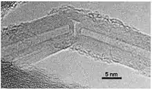
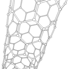
Junctions between two or more nanotubes have been widely discussed theoretically.[31][32] Such junctions are quite frequently observed in samples prepared by arc discharge as well as by chemical vapor deposition. The electronic properties of such junctions were first considered theoretically by Lambin et al.,[33] who pointed out that a connection between a metallic tube and a semiconducting one would represent a nanoscale heterojunction. Such a junction could therefore form a component of a nanotube-based electronic circuit. The adjacent image shows a junction between two multiwalled nanotubes.
Junctions between nanotubes and graphene have been considered theoretically[34] and studied experimentally.[35] Nanotube-graphene junctions form the basis of pillared graphene, in which parallel graphene sheets are separated by short nanotubes.[36] Pillared graphene represents a class of three-dimensional carbon nanotube architectures.
Recently, several studies have highlighted the prospect of using carbon nanotubes as building blocks to fabricate three-dimensional macroscopic (>100 nm in all three dimensions) all-carbon devices. Lalwani et al. have reported a novel radical-initiated thermal crosslinking method to fabricate macroscopic, free-standing, porous, all-carbon scaffolds using single- and multi-walled carbon nanotubes as building blocks.[37] These scaffolds possess macro-, micro-, and nano-structured pores, and the porosity can be tailored for specific applications. These 3D all-carbon scaffolds/architectures may be used for the fabrication of the next generation of energy storage, supercapacitors, field emission transistors, high-performance catalysis, photovoltaics, and biomedical devices, implants, and sensors.[38][39]
Other morphologies
Carbon nanobuds are a newly created material combining two previously discovered allotropes of carbon: carbon nanotubes and fullerenes. In this new material, fullerene-like "buds" are covalently bonded to the outer sidewalls of the underlying carbon nanotube. This hybrid material has useful properties of both fullerenes and carbon nanotubes. In particular, they have been found to be exceptionally good field emitters.[40] In composite materials, the attached fullerene molecules may function as molecular anchors preventing slipping of the nanotubes, thus improving the composite's mechanical properties.
A carbon peapod[41][42] is a novel hybrid carbon material which traps fullerene inside a carbon nanotube. It can possess interesting magnetic properties with heating and irradiation. It can also be applied as an oscillator during theoretical investigations and predictions.[43][44]
In theory, a nanotorus is a carbon nanotube bent into a torus (doughnut shape). Nanotori are predicted to have many unique properties, such as magnetic moments 1000 times larger than that previously expected for certain specific radii.[45] Properties such as magnetic moment, thermal stability, etc. vary widely depending on the radius of the torus and the radius of the tube.[45][46]
Graphenated carbon nanotubes are a relatively new hybrid that combines graphitic foliates grown along the sidewalls of multiwalled or bamboo style CNTs. The foliate density can vary as a function of deposition conditions (e.g., temperature and time) with their structure ranging from a few layers of graphene (< 10) to thicker, more graphite-like.[47] The fundamental advantage of an integrated graphene-CNT structure is the high surface area three-dimensional framework of the CNTs coupled with the high edge density of graphene. Depositing a high density of graphene foliates along the length of aligned CNTs can significantly increase the total charge capacity per unit of nominal area as compared to other carbon nanostructures.[48]
Cup-stacked carbon nanotubes (CSCNTs) differ from other quasi-1D carbon structures, which normally behave as quasi-metallic conductors of electrons. CSCNTs exhibit semiconducting behavior because of the stacking microstructure of graphene layers.[49]
Properties
Many properties of single-walled carbon nanotubes depend significantly on the (n,m) type, and this dependence is non-monotonic (see Kataura plot). In particular, the band gap can vary from zero to about 2 eV and the electrical conductivity can show metallic or semiconducting behavior.
Mechanical
Carbon nanotubes are the strongest and stiffest materials yet discovered in terms of tensile strength and elastic modulus. This strength results from the covalent sp2 bonds formed between the individual carbon atoms. In 2000, a multiwalled carbon nanotube was tested to have a tensile strength of 63 gigapascals (9,100,000 psi).[50] (For illustration, this translates into the ability to endure tension of a weight equivalent to 6,422 kilograms-force (62,980 N; 14,160 lbf) on a cable with cross-section of 1 square millimetre (0.0016 sq in)). Further studies, such as one conducted in 2008, revealed that individual CNT shells have strengths of up to ≈100 gigapascals (15,000,000 psi), which is in agreement with quantum/atomistic models.[51] Because carbon nanotubes have a low density for a solid of 1.3 to 1.4 g/cm3,[52] its specific strength of up to 48,000 kN·m·kg−1 is the best of known materials, compared to high-carbon steel's 154 kN·m·kg−1.
Although the strength of individual CNT shells is extremely high, weak shear interactions between adjacent shells and tubes lead to significant reduction in the effective strength of multiwalled carbon nanotubes and carbon nanotube bundles down to only a few GPa.[53] This limitation has been recently addressed by applying high-energy electron irradiation, which crosslinks inner shells and tubes, and effectively increases the strength of these materials to ≈60 GPa for multiwalled carbon nanotubes[51] and ≈17 GPa for double-walled carbon nanotube bundles.[53] CNTs are not nearly as strong under compression. Because of their hollow structure and high aspect ratio, they tend to undergo buckling when placed under compressive, torsional, or bending stress.[54]
On the other hand, there was evidence that in the radial direction they are rather soft. The first transmission electron microscope observation of radial elasticity suggested that even van der Waals forces can deform two adjacent nanotubes. Later, nanoindentations with an atomic force microscope were performed by several groups to quantitatively measure radial elasticity of multiwalled carbon nanotubes and tapping/contact mode atomic force microscopy was also performed on single-walled carbon nanotubes. Young's modulus of on the order of several GPa showed that CNTs are in fact very soft in the radial direction.
Electrical
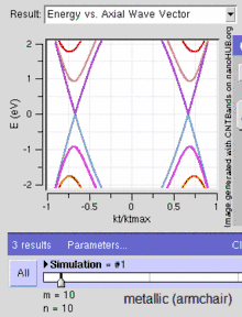
Unlike graphene, which is a two-dimensional semimetal, carbon nanotubes are either metallic or semiconducting along the tubular axis. For a given (n,m) nanotube, if n = m, the nanotube is metallic; if n − m is a multiple of 3 and n ≠ m and nm ≠ 0, then the nanotube is quasi-metallic with a very small band gap, otherwise the nanotube is a moderate semiconductor.[55] Thus, all armchair (n = m) nanotubes are metallic, and nanotubes (6,4), (9,1), etc. are semiconducting.[56] Carbon nanotubes are not semimetallic because the degenerate point (the point where the π [bonding] band meets the π* [anti-bonding] band, at which the energy goes to zero) is slightly shifted away from the K point in the Brillouin zone because of the curvature of the tube surface, causing hybridization between the σ* and π* anti-bonding bands, modifying the band dispersion.
The rule regarding metallic versus semiconductor behavior has exceptions because curvature effects in small-diameter tubes can strongly influence electrical properties. Thus, a (5,0) SWCNT that should be semiconducting in fact is metallic according to the calculations. Likewise, zigzag and chiral SWCNTs with small diameters that should be metallic have a finite gap (armchair nanotubes remain metallic).[56] In theory, metallic nanotubes can carry an electric current density of 4 × 10⁹ A/cm2, which is more than 1,000 times greater than those of metals such as copper,[57] where for copper interconnects, current densities are limited by electromigration. Carbon nanotubes are thus being explored as interconnects and conductivity-enhancing components in composite materials, and many groups are attempting to commercialize highly conducting electrical wire assembled from individual carbon nanotubes. There are significant challenges to be overcome however, such as undesired current saturation under voltage,[58] and the much more resistive nanotube-to-nanotube junctions and impurities, all of which lower the electrical conductivity of the macroscopic nanotube wires by orders of magnitude, as compared to the conductivity of the individual nanotubes.
Because of its nanoscale cross-section, electrons propagate only along the tube's axis. As a result, carbon nanotubes are frequently referred to as one-dimensional conductors. The maximum electrical conductance of a single-walled carbon nanotube is 2G0, where G0 = 2e2/h is the conductance of a single ballistic quantum channel.[59]
Because of the role of the π-electron system in determining the electronic properties of graphene, doping in carbon nanotubes differs from that of bulk crystalline semiconductors from the same group of the periodic table (e.g., silicon). Graphitic substitution of carbon atoms in the nanotube wall by boron or nitrogen dopants leads to p-type and n-type behavior, respectively, as would be expected in silicon. However, some non-substitutional (intercalated or adsorbed) dopants introduced into a carbon nanotube, such as alkali metals and electron-rich metallocenes, result in n-type conduction because they donate electrons to the π-electron system of the nanotube. By contrast, π-electron acceptors such as FeCl3 or electron-deficient metallocenes function as p-type dopants because they draw π-electrons away from the top of the valence band.
Intrinsic superconductivity has been reported,[60] although other experiments found no evidence of this, leaving the claim a subject of debate.[61]
Optical
Carbon nanotubes have useful absorption, photoluminescence (fluorescence), and Raman spectroscopy properties. Spectroscopic methods offer the possibility of quick and non-destructive characterization of relatively large amounts of carbon nanotubes. There is a strong demand for such characterization from the industrial point of view: numerous parameters of nanotube synthesis can be changed, intentionally or unintentionally, to alter the nanotube quality. As shown below, optical absorption, photoluminescence, and Raman spectroscopies allow quick and reliable characterization of this "nanotube quality" in terms of non-tubular carbon content, structure (chirality) of the produced nanotubes, and structural defects. These features determine nearly any other properties such as optical, mechanical, and electrical properties.
Carbon nanotubes are unique "one-dimensional systems" which can be envisioned as rolled single sheets of graphite (or more precisely graphene). This rolling can be done at different angles and curvatures resulting in different nanotube properties. The diameter typically varies in the range 0.4–40 nm (i.e., "only" ~100 times), but the length can vary ~100,000,000,000 times, from 0.14 nm to 55.5 cm.[62] The nanotube aspect ratio, or the length-to-diameter ratio, can be as high as 132,000,000:1,[63] which is unequalled by any other material. Consequently, all the properties of the carbon nanotubes relative to those of typical semiconductors are extremely anisotropic (directionally dependent) and tunable.
Whereas mechanical, electrical, and electrochemical (supercapacitor) properties of the carbon nanotubes are well established and have immediate applications, the practical use of optical properties is yet unclear. The aforementioned tunability of properties is potentially useful in optics and photonics. In particular, light-emitting diodes (LEDs)[64][65] and photo-detectors[66] based on a single nanotube have been produced in the lab. Their unique feature is not the efficiency, which is yet relatively low, but the narrow selectivity in the wavelength of emission and detection of light and the possibility of its fine tuning through the nanotube structure. In addition, bolometer[67] and optoelectronic memory[68] devices have been realised on ensembles of single-walled carbon nanotubes.
Crystallographic defects also affect the tube's electrical properties. A common result is lowered conductivity through the defective region of the tube. A defect in armchair-type tubes (which can conduct electricity) can cause the surrounding region to become semiconducting, and single monatomic vacancies induce magnetic properties.[69]
Thermal
All nanotubes are expected to be very good thermal conductors along the tube, exhibiting a property known as "ballistic conduction", but good insulators lateral to the tube axis. Measurements show that an individual SWNT has a room-temperature thermal conductivity along its axis of about 3500 W·m−1·K−1;[70] compare this to copper, a metal well known for its good thermal conductivity, which transmits 385 W·m−1·K−1. An individual SWNT has a room-temperature thermal conductivity lateral to its axis (in the radial direction) of about 1.52 W·m−1·K−1,[71] which is about as thermally conductive as soil. Macroscopic assemblies of nanotubes such as films or fibres have reached up to 1500 W·m−1·K−1 so far.[72] Networks composed of nanotubes demonstrate different values of thermal conductivity, from the level of thermal insulation with the thermal conductivity of 0.1 W·m−1·K−1 to such high values.[73] That is dependent on the amount of contribution to the thermal resistance of the system caused by the presence of impurities, misalignments and other factors. The temperature stability of carbon nanotubes is estimated to be up to 2800 °C in vacuum and about 750 °C in air.[74]
Crystallographic defects strongly affect the tube's thermal properties. Such defects lead to phonon scattering, which in turn increases the relaxation rate of the phonons. This reduces the mean free path and reduces the thermal conductivity of nanotube structures. Phonon transport simulations indicate that substitutional defects such as nitrogen or boron will primarily lead to scattering of high-frequency optical phonons. However, larger-scale defects such as Stone Wales defects cause phonon scattering over a wide range of frequencies, leading to a greater reduction in thermal conductivity.[75]
Synthesis
Techniques have been developed to produce nanotubes in sizable quantities, including arc discharge, laser ablation, chemical vapor deposition (CVD) and high-pressure carbon monoxide disproportionation (HiPCO). Among these arc discharge, laser ablation, chemical vapor deposition (CVD) are batch by batch process and HiPCO is gas phase continuous process.[76] Most of these processes take place in a vacuum or with process gases. The CVD growth method is popular, as it yields high quantity and has a degree of control over diameter, length and morphology. Using particulate catalysts, large quantities of nanotubes can be synthesized by these methods, but achieving the repeatability becomes a major problem with CVD growth.[77] The HiPCO process advances in catalysis and continuous growth are making CNTs more commercially viable.[78] The HiPCO process helps in producing high purity single walled carbon nanotubes in higher quantity. The HiPCO reactor operates at high temperature 900-1100 °C and high pressure ~30-50 bar.[79] It uses carbon monoxide as the carbon source and Iron pentacarbonyl or Nickel tetracarbonyl as a catalyst. These catalyst acts as the nucleation site for the nanotubes to grow.[76]
Vertically aligned carbon nanotube arrays are also grown by thermal chemical vapor deposition. A substrate (quartz, silicon, stainless steel, etc.) is coated with a catalytic metal (Fe, Co, Ni) layer. Typically that layer is iron, and is deposited via sputtering to a thickness of 1–5 nm. A 10–50 nm underlayer of alumina is often also put down on the substrate first. This imparts controllable wetting and good interfacial properties. When the substrate is heated to the growth temperature (~700 °C), the continuous iron film breaks up into small islands... each island then nucleates a carbon nanotube. The sputtered thickness controls the island size, and this in turn determines the nanotube diameter. Thinner iron layers drive down the diameter of the islands, and they drive down the diameter of the nanotubes grown. The amount of time that the metal island can sit at the growth temperature is limited, as they are mobile, and can merge into larger (but fewer) islands. Annealing at the growth temperature reduces the site density (number of CNT/mm2) while increasing the catalyst diameter.
The as-prepared carbon nanotubes always have impurities such as other forms of carbon (amorphous carbon, fullerene, etc.) and non-carbonaceous impurities (metal used for catalyst).[80][81] These impurities need to be removed to make use of the carbon nanotubes in applications.[82]
Modeling
Carbon nanotubes are modelled in a similar manner as traditional composites in which a reinforcement phase is surrounded by a matrix phase. Ideal models such as cylindrical, hexagonal and square models are common. The size of the micromechanics model is highly function of the studied mechanical properties. The concept of representative volume element (RVE) is used to determine the appropriate size and configuration of computer model to replicate the actual behavior of CNT reinforced nanocomposite. Depending on the material property of interest (thermal, electrical, modulus, creep), one RVE might predict the property better than the alternatives. While the implementation of ideal model is computationally efficient, they do not represent microstructural features observed in scanning electron microscopy of actual nanocomposites. To incorporate realistic modeling, computer models are also generated to incorporate variability such as waviness, orientation and agglomeration of multiwall or single wall carbon nanotubes.[83]
Metrology
There are many metrology standards and reference materials available for carbon nanotubes.[84]
For single-wall carbon nanotubes, ISO/TS 10868 describes a measurement method for the diameter, purity, and fraction of metallic nanotubes through optical absorption spectroscopy,[85] while ISO/TS 10797 and ISO/TS 10798 establish methods to characterize the morphology and elemental composition of single-wall carbon nanotubes, using transmission electron microscopy and scanning electron microscopy respectively, coupled with energy dispersive X-ray spectrometry analysis.[86][87]
NIST SRM 2483 is a soot of single-wall carbon nanotubes used as a reference material for elemental analysis, and was characterized using thermogravimetric analysis, prompt gamma activation analysis, induced neutron activation analysis, inductively coupled plasma mass spectroscopy, resonant Raman scattering, UV-visible-near infrared fluorescence spectroscopy and absorption spectroscopy, scanning electron microscopy, and transmission electron microscopy.[88][89] The Canadian National Research Council also offers a certified reference material SWCNT-1 for elemental analysis using neutron activation analysis and inductively coupled plasma mass spectroscopy.[84][90] NIST RM 8281 is a mixture of three lengths of single-wall carbon nanotube.[88][91]
For multiwall carbon nanotubes, ISO/TR 10929 identifies the basic properties and the content of impurities,[92] while ISO/TS 11888 describes morphology using scanning electron microscopy, transmission electron microscopy, viscometry, and light scattering analysis.[93] ISO/TS 10798 is also valid for multiwall carbon nanotubes.[87]
Chemical modification
Carbon nanotubes can be functionalized to attain desired properties that can be used in a wide variety of applications. The two main methods of carbon nanotube functionalization are covalent and non-covalent modifications. Because of their apparent hydrophobic nature,[94] carbon nanotubes tend to agglomerate hindering their dispersion in solvents or viscous polymer melts. The resulting nanotube bundles or aggregates reduce the mechanical performance of the final composite. The surface of the carbon nanotubes can be modified to reduce the hydrophobicity and improve interfacial adhesion to a bulk polymer through chemical attachment.[95]
The surface of carbon nanotubes can be chemically modified by coating spinel nanoparticles by hydrothermal synthesis[96] and can be used for water oxidation purposes.[97]
In addition, the surface of carbon nanotubes can be fluorinated or halofluorinated by heating while in contact with a fluoroorganic substance, thereby forming partially fluorinated carbons (so called Fluocar materials) with grafted (halo)fluoroalkyl functionality.[98][99]
Applications
A primary obstacle for applications of carbon nanotubes has been their cost. Prices for single-walled nanotubes declined from around $1500 per gram as of 2000 to retail prices of around $50 per gram of as-produced 40–60% by weight SWNTs as of March 2010. As of 2016, the retail price of as-produced 75% by weight SWNTs was $2 per gram.[100] SWNTs are forecast to make a large impact in electronics applications by 2020 according to The Global Market for Carbon Nanotubes report.
Current
Current use and application of nanotubes has mostly been limited to the use of bulk nanotubes, which is a mass of rather unorganized fragments of nanotubes. Bulk nanotube materials may never achieve a tensile strength similar to that of individual tubes, but such composites may, nevertheless, yield strengths sufficient for many applications. Bulk carbon nanotubes have already been used as composite fibers in polymers to improve the mechanical, thermal and electrical properties of the bulk product.
- Easton-Bell Sports, Inc. have been in partnership with Zyvex Performance Materials, using CNT technology in a number of their bicycle components – including flat and riser handlebars, cranks, forks, seatposts, stems and aero bars.
- Amroy Europe Oy manufactures Hybtonite carbon nanoepoxy resins where carbon nanotubes have been chemically activated to bond to epoxy, resulting in a composite material that is 20% to 30% stronger than other composite materials. It has been used for wind turbines, marine paints and a variety of sports gear such as skis, ice hockey sticks, baseball bats, hunting arrows, and surfboards.[101]
- Surrey NanoSystems synthesises carbon nanotubes to create vantablack.
Other current applications include:
- tips for atomic force microscope probes[102]
- in tissue engineering, carbon nanotubes can act as scaffolding for bone growth[103]
Under development
Current research for modern applications include:
- Utilizing carbon nanotubes as the channel material of carbon nanotube field-effect transistors.[104]
- Using carbon nanotubes as a scaffold for diverse microfabrication techniques.[105]
- Energy dissipation in self-organized nanostructures under influence of an electric field.[106]
- Using carbon nanotubes for environmental monitoring due to their active surface area and their ability to absorb gases.[107]
- Jack Andraka used carbon nanotubes in his pancreatic cancer test. His method of testing won the Intel International Science and Engineering Fair Gordon E. Moore Award in the spring of 2012.Jack Andraka, the Teen Prodigy of Pancreatic Cancer
- The Boeing Company has patented the use of carbon nanotubes for structural health monitoring[108] of composites used in aircraft structures. This technology will greatly reduce the risk of an in-flight failure caused by structural degradation of aircraft.
- Zyvex Technologies has also built a 54' maritime vessel, the Piranha Unmanned Surface Vessel, as a technology demonstrator for what is possible using CNT technology. CNTs help improve the structural performance of the vessel, resulting in a lightweight 8,000 lb boat that can carry a payload of 15,000 lb over a range of 2,500 miles.[109]
Carbon nanotubes can serve as additives to various structural materials. For instance, nanotubes form a tiny portion of the material(s) in some (primarily carbon fiber) baseball bats, golf clubs, car parts, or damascus steel.[110][111]
IBM expected carbon nanotube transistors to be used on Integrated Circuits by 2020.[112]
Potential
The strength and flexibility of carbon nanotubes makes them of potential use in controlling other nanoscale structures, which suggests they will have an important role in nanotechnology engineering.[113] The highest tensile strength of an individual multi-walled carbon nanotube has been tested to be 63 GPa.[50] Carbon nanotubes were found in Damascus steel from the 17th century, possibly helping to account for the legendary strength of the swords made of it.[114][115] Recently, several studies have highlighted the prospect of using carbon nanotubes as building blocks to fabricate three-dimensional macroscopic (>1mm in all three dimensions) all-carbon devices. Lalwani et al. have reported a novel radical initiated thermal crosslinking method to fabricated macroscopic, free-standing, porous, all-carbon scaffolds using single- and multi-walled carbon nanotubes as building blocks.[37] These scaffolds possess macro-, micro-, and nano- structured pores and the porosity can be tailored for specific applications. These 3D all-carbon scaffolds/architectures may be used for the fabrication of the next generation of energy storage, supercapacitors, field emission transistors, high-performance catalysis,[116] photovoltaics, and biomedical devices and implants.
CNTs are potential candidates for future via and wire material in nano-scale VLSI circuits. Eliminating electromigration reliability concerns that plague today's Cu interconnects, isolated (single and multi-wall) CNTs can carry current densities in excess of 1000 MA/cm2 without electromigration damage.[117]
Single-walled nanotubes are likely candidates for miniaturizing electronics. The most basic building block of these systems is an electric wire, and SWNTs with diameters of an order of a nanometer can be excellent conductors.[118][119] One useful application of SWNTs is in the development of the first intermolecular field-effect transistors (FET). The first intermolecular logic gate using SWCNT FETs was made in 2001.[120] A logic gate requires both a p-FET and an n-FET. Because SWNTs are p-FETs when exposed to oxygen and n-FETs otherwise, it is possible to expose half of an SWNT to oxygen and protect the other half from it. The resulting SWNT acts as a not logic gate with both p- and n-type FETs in the same molecule.
Large quantities of pure CNTs can be made into a freestanding sheet or film by surface-engineered tape-casting (SETC) fabrication technique which is a scalable method to fabricate flexible and foldable sheets with superior properties.[121][122] Another reported form factor is CNT fiber (a.k.a. filament) by wet spinning.[123] The fiber is either directly spun from the synthesis pot or spun from pre-made dissolved CNTs. Individual fibers can be turned into a yarn. Apart from its strength and flexibility, the main advantage is making an electrically conducting yarn. The electronic properties of individual CNT fibers (i.e. bundle of individual CNT) are governed by the two-dimensional structure of CNTs. The fibers were measured to have a resistivity only one order of magnitude higher than metallic conductors at 300K. By further optimizing the CNTs and CNT fibers, CNT fibers with improved electrical properties could be developed.[117][124]
CNT-based yarns are suitable for applications in energy and electrochemical water treatment when coated with an ion-exchange membrane.[125] Also, CNT-based yarns could replace copper as a winding material. Pyrhönen et al. (2015) have built a motor using CNT winding.[126][127]
Safety and health
The National Institute for Occupational Safety and Health (NIOSH) is the leading United States federal agency conducting research and providing guidance on the occupational safety and health implications and applications of nanotechnology. Early scientific studies have indicated that some of these nanoscale particles may pose a greater health risk than the larger bulk form of these materials. In 2013, NIOSH published a Current Intelligence Bulletin detailing the potential hazards and recommended exposure limit for carbon nanotubes and fibers.[128]
As of October 2016, single wall carbon nanotubes have been registered through the European Union's Registration, Evaluation, Authorization and Restriction of Chemicals (REACH) regulations, based on evaluation of the potentially hazardous properties of SWCNT. Based on this registration, SWCNT commercialization is allowed in the EU up to 10 metric tons. Currently, the type of SWCNT registered through REACH is limited to the specific type of single wall carbon nanotubes manufactured by OCSiAl, which submitted the application.[129]
History
The true identity of the discoverers of carbon nanotubes is a subject of some controversy.[130] A 2006 editorial written by Marc Monthioux and Vladimir Kuznetsov in the journal Carbon described the interesting and often-misstated origin of the carbon nanotube.[6] A large percentage of academic and popular literature attributes the discovery of hollow, nanometer-size tubes composed of graphitic carbon to Sumio Iijima of NEC in 1991. He published a paper describing his discovery which initiated a flurry of excitement and could be credited by inspiring the many scientists now studying applications of carbon nanotubes. Though Iijima has been given much of the credit for discovering carbon nanotubes, it turns out that the timeline of carbon nanotubes goes back much further than 1991.[130]
In 1952, L. V. Radushkevich and V. M. Lukyanovich published clear images of 50 nanometer diameter tubes made of carbon in the Soviet Journal of Physical Chemistry.[5] This discovery was largely unnoticed, as the article was published in Russian, and Western scientists' access to Soviet press was limited during the Cold War. Monthioux and Kuznetsov mentioned in their Carbon editorial:[6]
The fact is, Radushkevich and Lukyanovich [..] should be credited for the discovery that carbon filaments could be hollow and have a nanometer- size diameter, that is to say for the discovery of carbon nanotubes.
In 1976, Morinobu Endo of CNRS observed hollow tubes of rolled up graphite sheets synthesised by a chemical vapour-growth technique.[4] The first specimens observed would later come to be known as single-walled carbon nanotubes (SWNTs).[131] Endo, in his early review of vapor-phase-grown carbon fibers (VPCF), also reminded us that he had observed a hollow tube, linearly extended with parallel carbon layer faces near the fiber core.[132] This appears to be the observation of multi-walled carbon nanotubes at the center of the fiber.[131] The mass-produced MWCNTs today are strongly related to the VPGCF developed by Endo.[131] In fact, they call it the "Endo-process", out of respect for his early work and patents.[131][133]
In 1979, John Abrahamson presented evidence of carbon nanotubes at the 14th Biennial Conference of Carbon at Pennsylvania State University. The conference paper described carbon nanotubes as carbon fibers that were produced on carbon anodes during arc discharge. A characterization of these fibers was given as well as hypotheses for their growth in a nitrogen atmosphere at low pressures.[134]
In 1981, a group of Soviet scientists published the results of chemical and structural characterization of carbon nanoparticles produced by a thermocatalytical disproportionation of carbon monoxide. Using TEM images and XRD patterns, the authors suggested that their "carbon multi-layer tubular crystals" were formed by rolling graphene layers into cylinders. They speculated that by rolling graphene layers into a cylinder, many different arrangements of graphene hexagonal nets are possible. They suggested two possibilities of such arrangements: circular arrangement (armchair nanotube) and a spiral, helical arrangement (chiral tube).[135]
In 1987, Howard G. Tennent of Hyperion Catalysis was issued a U.S. patent for the production of "cylindrical discrete carbon fibrils" with a "constant diameter between about 3.5 and about 70 nanometers..., length 102 times the diameter, and an outer region of multiple essentially continuous layers of ordered carbon atoms and a distinct inner core...."[136]
Iijima's discovery of multi-walled carbon nanotubes in the insoluble material of arc-burned graphite rods in 1991[3] and Mintmire, Dunlap, and White's independent prediction that if single-walled carbon nanotubes could be made, then they would exhibit remarkable conducting properties[7] helped create the initial excitement associated with carbon nanotubes. Nanotube research accelerated greatly following the independent discoveries[1][2] by Iijima and Ichihashi at NEC and Bethune et al. at IBM of single-walled carbon nanotubes and methods to specifically produce them by adding transition-metal catalysts to the carbon in an arc discharge. The arc discharge technique was well known to produce the famed Buckminster fullerene on a preparative scale,[137] and these results appeared to extend the run of accidental discoveries relating to fullerenes. The discovery of nanotubes remains a contentious issue. Many believe that Iijima's report in 1991 is of particular importance because it brought carbon nanotubes into the awareness of the scientific community as a whole.[130][131]
Keezhadi in Tamilnadu, India excavation commenced in 2014, so far has done at six phases and the majority of excavations were artifacts and potteries. After the sixth phase of excavation, completed in October 2020, nanotechnology usage in Keezhadi was found out and it is claimed that it is the first time that usage of nanotechnology was found out before 2,500 years ago. The articles published in scientific journals said coatings on top of the potteries excavated from Keezhadi contains carbon nanotubes. The robust mechanical properties of carbon nanotubes the coatings have lasted for so many years, says the Scientists.[138]
See also
- BCN nanotube
- Boron nitride nanotube
- Buckypaper
- Carbide-derived carbon
- Carbon nanocone
- Carbon nanofibers
- Carbon nanoparticles
- Carbon nanoscrolls
- Carbon nanotube chemistry
- Carbon nanotube computer
- Carbon nanotube field-effect transistor
- Colossal carbon tube
- Diamond nanothread
- DNA nanotube
- Filamentous carbon
- Gallium nitride nanotube
- Geodesic polyarene
- Graphene oxide paper
- Inorganic nanotube
- List of software for nanostructures modeling
- Molecular modelling
- Nanoflower
- Nitrogen-doped carbon nanotube
- Ninithi (nanotube modelling software)
- Organic semiconductor
- SAMSON (software platform for integrated computational nanoscience)
- Selective chemistry of single-walled nanotubes
- Silicon nanotubes
- Timeline of carbon nanotubes
- Titania nanotubes
- Tunneling nanotube
- Tungsten(IV) sulfide Nanotubes
- Vertically aligned carbon nanotube arrays
References
This article incorporates public domain text from National Institute of Environmental Health Sciences (NIEHS) as quoted.
- Iijima, Sumio; Ichihashi, Toshinari (17 June 1993). "Single-shell carbon nanotubes of 1-nm diameter". Nature. 363 (6430): 603–605. Bibcode:1993Natur.363..603I. doi:10.1038/363603a0. S2CID 4314177.
- Bethune, D. S.; Kiang, C. H.; De Vries, M. S.; Gorman, G.; Savoy, R.; Vazquez, J.; Beyers, R. (17 June 1993). "Cobalt-catalyzed growth of carbon nanotubes with single-atomic-layer walls". Nature. 363 (6430): 605–607. Bibcode:1993Natur.363..605B. doi:10.1038/363605a0. S2CID 4321984.
- Iijima, Sumio (7 November 1991). "Helical microtubules of graphitic carbon". Nature. 354 (6348): 56–58. Bibcode:1991Natur.354...56I. doi:10.1038/354056a0. S2CID 4302490.
- Oberlin, A.; Endo, M.; Koyama, T. (March 1976). "Filamentous growth of carbon through benzene decomposition". Journal of Crystal Growth. 32 (3): 335–349. Bibcode:1976JCrGr..32..335O. doi:10.1016/0022-0248(76)90115-9.
- Радушкевич, Л. В. (1952). "Archived copy" О Структуре Углерода, Образующегося При Термическом Разложении Окиси Углерода На Железном Контакте (PDF). Журнал Физической Химии (in Russian). 26: 88–95. Archived from the original (PDF) on 5 March 2016. Retrieved 5 April 2012.CS1 maint: archived copy as title (link)
- Monthioux, Marc; Kuznetsov, Vladimir L. (August 2006). "Who should be given the credit for the discovery of carbon nanotubes?" (PDF). Carbon. 44 (9): 1621–1623. doi:10.1016/j.carbon.2006.03.019.
- Mintmire, J.W.; Dunlap, B.I.; White, C.T. (3 February 1992). "Are fullerene tubules metallic?". Phys. Rev. Lett. 68 (5): 631–634. Bibcode:1992PhRvL..68..631M. doi:10.1103/PhysRevLett.68.631. PMID 10045950.
- Tans, Sander J.; Devoret, Michel H.; Dai, Hongjie; Thess, Andreas; Smalley, Richard E.; Geerligs, L. J.; Dekker, Cees (April 1997). "Individual single-wall carbon nanotubes as quantum wires". Nature. 386 (6624): 474–477. Bibcode:1997Natur.386..474T. doi:10.1038/386474a0. S2CID 4366705.
- Hamada, Noriaki; Sawada, Shin-ichi; Oshiyama, Atsushi (9 March 1992). "New one-dimensional conductors: Graphitic microtubules". Physical Review Letters. 68 (10): 1579–1581. Bibcode:1992PhRvL..68.1579H. doi:10.1103/PhysRevLett.68.1579. PMID 10045167.
- Wildoer, J.W.G.; Venema, L.C.; Rinzler, A.G.; Smalley, R.E.; Dekker, C. (1 January 1998). "Electronic structure of atomically resolved carbon nanotubes". Nature. 391 (6662): 59–62. Bibcode:1998Natur.391...59W. doi:10.1038/34139. S2CID 205003208.
- Yu, M.; Lourie, O; Dyer, MJ; Moloni, K; Kelly, TF; Ruoff, RS (28 January 2000). "Strength and Breaking Mechanism of Multiwalled Carbon Nanotubes Under Tensile Load". Science. 287 (5453): 637–640. Bibcode:2000Sci...287..637Y. doi:10.1126/science.287.5453.637. PMID 10649994.
- Berber, Savas; Kwon, Young-Kyun; Tománek, David (15 May 2000). "Unusually High Thermal Conductivity of Carbon Nanotubes". Physical Review Letters. 84 (20): 4613–4616. arXiv:cond-mat/0002414. Bibcode:2000PhRvL..84.4613B. doi:10.1103/PhysRevLett.84.4613. PMID 10990753. S2CID 9006722.
- Kim, P.; Shi, L.; Majumdar, A.; McEuen, P. L. (31 October 2001). "Thermal Transport Measurements of Individual Multiwalled Nanotubes". Physical Review Letters. 87 (21): 215502. arXiv:cond-mat/0106578. Bibcode:2001PhRvL..87u5502K. doi:10.1103/PhysRevLett.87.215502. PMID 11736348. S2CID 12533685.
- Karousis, Nikolaos; Tagmatarchis, Nikos; Tasis, Dimitrios (8 September 2010). "Current Progress on the Chemical Modification of Carbon Nanotubes". Chemical Reviews. 110 (9): 5366–5397. doi:10.1021/cr100018g. PMID 20545303.
- S. B. Sinnott & R. Andreys (2001). "Carbon Nanotubes: Synthesis, Properties, and Applications". Critical Reviews in Solid State and Materials Sciences. 26 (3): 145–249. Bibcode:2001CRSSM..26..145S. doi:10.1080/20014091104189. S2CID 95444574.
- Zhao, X.; Liu, Y.; Inoue, S.; Suzuki, T.; Jones, R.; Ando, Y. (2004). "Smallest Carbon Nanotube is 3 Å in Diameter" (PDF). Phys. Rev. Lett. 92 (12): 125502. Bibcode:2004PhRvL..92l5502Z. doi:10.1103/PhysRevLett.92.125502. PMID 15089683.
- Torres-Dias, Abraao C. (2017). "From mesoscale to nanoscale mechanics in single-wall carbon nanotubes". Carbon. 123: 145–150. doi:10.1016/j.carbon.2017.07.036.
- Hayashi, Takuya; Kim, Yoong Ahm; Matoba, Toshiharu; Esaka, Masaya; Nishimura, Kunio; Tsukada, Takayuki; Endo, Morinobu; Dresselhaus, Mildred S. (2003). "Smallest Freestanding Single-Walled Carbon Nanotube". Nano Letters. 3 (7): 887–889. Bibcode:2003NanoL...3..887H. doi:10.1021/nl034080r.
- Guan, L.; Suenaga, K.; Iijima, S. (2008). "Smallest Carbon Nanotube Assigned with Atomic Resolution Accuracy". Nano Letters. 8 (2): 459–462. Bibcode:2008NanoL...8..459G. doi:10.1021/nl072396j. PMID 18186659.
- Zhang, Rufan; Zhang, Yingying; Zhang, Qiang; Xie, Huanhuan; Qian, Weizhong; Wei, Fei (23 July 2013). "Growth of Half-Meter Long Carbon Nanotubes Based on Schulz–Flory Distribution". ACS Nano. 7 (7): 6156–6161. doi:10.1021/nn401995z. PMID 23806050.
- Wang, X.; Li, Qunqing; Xie, Jing; Jin, Zhong; Wang, Jinyong; Li, Yan; Jiang, Kaili; Fan, Shoushan (2009). "Fabrication of Ultralong and Electrically Uniform Single-Walled Carbon Nanotubes on Clean Substrates". Nano Letters. 9 (9): 3137–3141. Bibcode:2009NanoL...9.3137W. CiteSeerX 10.1.1.454.2744. doi:10.1021/nl901260b. PMID 19650638.
- Jasti, Ramesh; Bhattacharjee, Joydeep; Neaton, Jeffrey B; Bertozzi, Carolyn R (4 December 2008). "Synthesis, Characterization, and Theory of [9]-, [12]-, and [18]Cycloparaphenylene: Carbon Nanohoop Structures". Journal of the American Chemical Society. 130 (52): 17646–17647. doi:10.1021/ja807126u. PMC 2709987. PMID 19055403.
- Cheung, Kwan Yin; Segawa, Yasutomo; Itami, Kenichiro (2020). "Synthetic Strategies of Carbon Nanobelts and Related Belt-Shaped Polycyclic Aromatic Hydrocarbons". Chemistry – A European Journal. 26 (65): 14791–14801. doi:10.1002/chem.202002316. ISSN 1521-3765.
- "Densest array of carbon nanotubes grown to date". KurzweilAI. 27 September 2013.
- Sugime, H.; Esconjauregui, S.; Yang, J.; d'Arsié, L.; Oliver, R. A.; Bhardwaj, S.; Cepek, C.; Robertson, J. (2013). "Low temperature growth of ultra-high mass density carbon nanotube forests on conductive supports". Applied Physics Letters. 103 (7): 073116. Bibcode:2013ApPhL.103g3116S. doi:10.1063/1.4818619.
- Das, Sudip (March 2013). "A review on Carbon nano-tubes – A new era of nanotechnology" (PDF). International Journal of Emerging Technology and Advanced Engineering. 3 (3): 774–781. CiteSeerX 10.1.1.413.7576.
- Flahaut, Emmanuel; Bacsa, Revathi; Peigney, Alain; Laurent, Christophe (2003). "Gram-scale CCVD synthesis of double-walled carbon nanotubes" (PDF). Chemical Communications (12): 1442–3. doi:10.1039/b301514a. PMID 12841282.
- Cumings, J.; Zettl, A. (2000). "Low-Friction Nanoscale Linear Bearing Realized from Multiwall Carbon Nanotubes". Science. 289 (5479): 602–604. Bibcode:2000Sci...289..602C. CiteSeerX 10.1.1.859.7671. doi:10.1126/science.289.5479.602. PMID 10915618.
- Treacy, M.M.J.; Ebbesen, T.W.; Gibson, J.M. (1996). "Exceptionally high Young's modulus observed for individual carbon nanotubes". Nature. 381 (6584): 678–680. Bibcode:1996Natur.381..678T. doi:10.1038/381678a0. S2CID 4332264.
- Zavalniuk, V.; Marchenko, S. (2011). "Theoretical analysis of telescopic oscillations in multi-walled carbon nanotubes" (PDF). Low Temperature Physics. 37 (4): 337–342. arXiv:0903.2461. Bibcode:2011LTP....37..337Z. doi:10.1063/1.3592692. S2CID 51932307.
- Chernozatonskii, L.A. (1992). "Carbon nanotube connectors and planar jungle gyms". Physics Letters A. 172 (3): 173–176. Bibcode:1992PhLA..172..173C. doi:10.1016/0375-9601(92)90978-u.
- Menon, Madhu; Srivastava, Deepak (1 December 1997). "Carbon Nanotube 'T Junctions': Nanoscale Metal-Semiconductor-Metal Contact Devices". Physical Review Letters. 79 (22): 4453–4456. Bibcode:1997PhRvL..79.4453M. doi:10.1103/physrevlett.79.4453.
- Lambin, P. (1996). "Atomic structure and electronic properties of bent carbon nanotubes". Synth. Met. 77 (1–3): 249–1254. doi:10.1016/0379-6779(96)80097-x.
- Ma, K.L. (2011). "Electronic transport properties of junctions between carbon nanotubes and graphene nanoribbons". European Physical Journal B. 83 (4): 487–492. Bibcode:2011EPJB...83..487M. doi:10.1140/epjb/e2011-20313-9. S2CID 119497542.
- Harris, P.J.F. (2016). "The structure of junctions between carbon nanotubes and graphene shells" (PDF). Nanoscale. 8 (45): 18849–18854. doi:10.1039/c6nr06461b. PMID 27808332.
- Dimitrakakis, G. K. (2008). "Pillared graphene: a new 3-D network nanostructure for enhanced hydrogen storage". Nano Lett. 8 (10): 3166–3170. Bibcode:2008NanoL...8.3166D. doi:10.1021/nl801417w. PMID 18800853.
- Lalwani, Gaurav; Kwaczala, Andrea Trinward; Kanakia, Shruti; Patel, Sunny C.; Judex, Stefan; Sitharaman, Balaji (March 2013). "Fabrication and characterization of three-dimensional macroscopic all-carbon scaffolds". Carbon. 53: 90–100. doi:10.1016/j.carbon.2012.10.035. PMC 3578711. PMID 23436939.
- Balaji Sitharaman., Lalwani, Gaurav, Anu Gopalan, Michael D'Agati, Jeyantt Srinivas Sankaran, Stefan Judex, Yi-Xian Qin (2015). "Porous three-dimensional carbon nanotube scaffolds for tissue engineering". Journal of Biomedical Materials Research Part A. 103 (10): 3212–3225. doi:10.1002/jbm.a.35449. PMC 4552611. PMID 25788440.
- Noyce, Steven G.; Vanfleet, Richard R.; Craighead, Harold G.; Davis, Robert C. (2019). "High surface-area carbon microcantilevers". Nanoscale Advances. 1 (3): 1148–1154. Bibcode:2019NanoA...1.1148N. doi:10.1039/C8NA00101D.
- Nasibulin, Albert G.; Pikhitsa, Peter V.; Jiang, Hua; Brown, David P.; Krasheninnikov, Arkady V.; Anisimov, Anton S.; Queipo, Paula; Moisala, Anna; Gonzalez, David; Lientschnig, Günther; Hassanien, Abdou; Shandakov, Sergey D.; Lolli, Giulio; Resasco, Daniel E.; Choi, Mansoo; Tománek, David; Kauppinen, Esko I. (March 2007). "A novel hybrid carbon material". Nature Nanotechnology. 2 (3): 156–161. Bibcode:2007NatNa...2..156N. doi:10.1038/nnano.2007.37. PMID 18654245.
- Smith, Brian W.; Monthioux, Marc; Luzzi, David E. (1998). "Encapsulated C-60 in carbon nanotubes". Nature. 396 (6709): 323–324. Bibcode:1998Natur.396R.323S. doi:10.1038/24521. S2CID 30670931.
- Smith, B.W.; Luzzi, D.E. (2000). "Formation mechanism of fullerene peapods and coaxial tubes: a path to large scale synthesis". Chem. Phys. Lett. 321 (1–2): 169–174. Bibcode:2000CPL...321..169S. doi:10.1016/S0009-2614(00)00307-9.
- Su, H.; Goddard, W.A.; Zhao, Y. (2006). "Dynamic friction force in a carbon peapod oscillator" (PDF). Nanotechnology. 17 (22): 5691–5695. arXiv:cond-mat/0611671. Bibcode:2006Nanot..17.5691S. doi:10.1088/0957-4484/17/22/026. S2CID 18165997.
- Wang, M.; Li, C.M. (2010). "An oscillator in a carbon peapod controllable by an external electric field: A molecular dynamics study". Nanotechnology. 21 (3): 035704. Bibcode:2010Nanot..21c5704W. doi:10.1088/0957-4484/21/3/035704. PMID 19966399.
- Liu, L.; Guo, G.; Jayanthi, C.; Wu, S. (2002). "Colossal Paramagnetic Moments in Metallic Carbon Nanotori". Phys. Rev. Lett. 88 (21): 217206. Bibcode:2002PhRvL..88u7206L. doi:10.1103/PhysRevLett.88.217206. PMID 12059501.
- Huhtala, M.; Kuronen, A.; Kaski, K. (2002). "Carbon nanotube structures: Molecular dynamics simulation at realistic limit" (PDF). Computer Physics Communications. 146 (1): 30–37. Bibcode:2002CoPhC.146...30H. doi:10.1016/S0010-4655(02)00432-0. Archived from the original (PDF) on 27 June 2008.
- Parker, Charles B.; Akshay S. Raut; Billyde Brown; Brian R. Stoner; Jeffrey T. Glass (2012). "Three-dimensional arrays of graphenated carbon nanotubes". J. Mater. Res. 7. 27 (7): 1046–1053. Bibcode:2012JMatR..27.1046P. doi:10.1557/jmr.2012.43.
- Stoner, Brian R.; Jeffrey T. Glass (2012). "Carbon nanostructures: a morphological classification for charge density optimization". Diamond and Related Materials. 23: 130–134. Bibcode:2012DRM....23..130S. doi:10.1016/j.diamond.2012.01.034.
- Liu, Q.; Ren, Wencai; Chen, Zhi-Gang; Yin, Lichang; Li, Feng; Cong, Hongtao; Cheng, Hui-Ming (2009). "Semiconducting properties of cup-stacked carbon nanotubes" (PDF). Carbon. 47 (3): 731–736. doi:10.1016/j.carbon.2008.11.005. Archived from the original (PDF) on 9 January 2015.
- Yu, M.; Lourie, O; Dyer, MJ; Moloni, K; Kelly, TF; Ruoff, RS (28 January 2000). "Strength and Breaking Mechanism of Multiwalled Carbon Nanotubes Under Tensile Load". Science. 287 (5453): 637–640. Bibcode:2000Sci...287..637Y. doi:10.1126/science.287.5453.637. PMID 10649994.
- Peng, Bei; Locascio, Mark; Zapol, Peter; Li, Shuyou; Mielke, Steven L.; Schatz, George C.; Espinosa, Horacio D. (October 2008). "Measurements of near-ultimate strength for multiwalled carbon nanotubes and irradiation-induced crosslinking improvements". Nature Nanotechnology. 3 (10): 626–631. doi:10.1038/nnano.2008.211. PMID 18839003.
- Collins, Philip G.; Avouris, Phaedon (December 2000). "Nanotubes for Electronics". Scientific American. 283 (6): 62–69. Bibcode:2000SciAm.283f..62C. doi:10.1038/scientificamerican1200-62. PMID 11103460.
- Filleter, T.; Bernal, R.; Li, S.; Espinosa, H.D. (5 July 2011). "Ultrahigh Strength and Stiffness in Cross-Linked Hierarchical Carbon Nanotube Bundles". Advanced Materials. 23 (25): 2855–2860. doi:10.1002/adma.201100547. PMID 21538593.
- Jensen, K.; Mickelson, W.; Kis, A.; Zettl, A. (26 November 2007). "Buckling and kinking force measurements on individual multiwalled carbon nanotubes". Physical Review B. 76 (19): 195436. Bibcode:2007PhRvB..76s5436J. doi:10.1103/PhysRevB.76.195436.
- Laird, Edward A.; Kuemmeth, Ferdinand; Steele, Gary A.; Grove-Rasmussen, Kasper; Nygård, Jesper; Flensberg, Karsten; Kouwenhoven, Leo P. (2015). "Quantum Transport in Carbon Nanotubes". Reviews of Modern Physics. 87 (3): 703–764. arXiv:1403.6113. Bibcode:2015RvMP...87..703L. doi:10.1103/RevModPhys.87.703. S2CID 119208985.
- Lu, X.; Chen, Z. (2005). "Curved Pi-Conjugation, Aromaticity, and the Related Chemistry of Small Fullerenes (C60) and Single-Walled Carbon Nanotubes". Chemical Reviews. 105 (10): 3643–3696. doi:10.1021/cr030093d. PMID 16218563.
- Hong, Seunghun; Myung, S (2007). "Nanotube Electronics: A flexible approach to mobility". Nature Nanotechnology. 2 (4): 207–208. Bibcode:2007NatNa...2..207H. doi:10.1038/nnano.2007.89. PMID 18654263.
- Vasylenko, Andrij; Wynn, Jamie; Medeiros, Paulo V. C.; Morris, Andrew J.; Sloan, Jeremy; Quigley, David (2017). "Encapsulated nanowires: Boosting electronic transport in carbon nanotubes". Physical Review B. 95 (12): 121408. arXiv:1611.04867. Bibcode:2017PhRvB..95l1408V. doi:10.1103/PhysRevB.95.121408. S2CID 59023024.
- Charlier, J. C.; Blase, X.; Roche, S. (2007). "Electronic and transport properties of nanotubes". Reviews of Modern Physics. 79 (2): 677–732. Bibcode:2007RvMP...79..677C. doi:10.1103/RevModPhys.79.677.
- Tang, Z. K.; Zhang, L; Wang, N; Zhang, XX; Wen, GH; Li, GD; Wang, JN; Chan, CT; Sheng, P (2001). "Superconductivity in 4 Angstrom Single-Walled Carbon Nanotubes". Science. 292 (5526): 2462–2465. Bibcode:2001Sci...292.2462T. doi:10.1126/science.1060470. PMID 11431560. S2CID 44987798.
Takesue, I.; Haruyama, J.; Kobayashi, N.; Chiashi, S.; Maruyama, S.; Sugai, T.; Shinohara, H. (2006). "Superconductivity in Entirely End-Bonded Multiwalled Carbon Nanotubes" (PDF). Phys. Rev. Lett. 96 (5): 057001. arXiv:cond-mat/0509466. Bibcode:2006PhRvL..96e7001T. doi:10.1103/PhysRevLett.96.057001. PMID 16486971. S2CID 119049151.
Lortz, R.; Zhang, Q; Shi, W; Ye, J. T.; Qiu, C. Y.; Wang, Z.; He, H. T.; Sheng, P; Qian, T. Z.; Tang, Z. K.; Wang, N.; Zhang, X. X.; Wang, J; Chan, C. T. (2009). "Superconducting characteristics of 4-A carbon nanotube–zeolite composite". Proceedings of the National Academy of Sciences. 106 (18): 7299–7303. Bibcode:2009PNAS..106.7299L. doi:10.1073/pnas.0813162106. PMC 2678622. PMID 19369206. - Bockrath, M. (2006). "Carbon nanotubes: The weakest link". Nature Physics. 2 (3): 155–156. Bibcode:2006NatPh...2..155B. doi:10.1038/nphys252. S2CID 125902065.
- Zhang, R.; Zhang, Y.; Zhang, Q.; Xie, H.; Qian, W.; Wei, F. (2013). "Growth of Half-Meter Long Carbon Nanotubes Based on Schulz–Flory Distribution". ACS Nano. 7 (7): 6156–6161. doi:10.1021/nn401995z. PMID 23806050.
- Xueshen Wang; et al. (2009). "Fabrication of Ultralong and Electrically Uniform Single-Walled Carbon Nanotubes on Clean Substrates" (PDF). Nano Letters. 9 (9): 3137–3141. Bibcode:2009NanoL...9.3137W. CiteSeerX 10.1.1.454.2744. doi:10.1021/nl901260b. PMID 19650638. Archived from the original (PDF) on 8 August 2017. Retrieved 24 October 2017.
- J. A. Misewich; et al. (2003). "Electrically Induced Optical Emission from a Carbon Nanotube FET". Science. 300 (5620): 783–786. Bibcode:2003Sci...300..783M. doi:10.1126/science.1081294. PMID 12730598. S2CID 36336745.
- J. Chen; et al. (2005). "Bright Infrared Emission from Electrically Induced Excitons in Carbon Nanotubes". Science. 310 (5751): 1171–1174. Bibcode:2005Sci...310.1171C. doi:10.1126/science.1119177. PMID 16293757. S2CID 21960183.
- M. Freitag; et al. (2003). "Photoconductivity of Single Carbon Nanotubes". Nano Letters. 3 (8): 1067–1071. Bibcode:2003NanoL...3.1067F. doi:10.1021/nl034313e.
- M. E. Itkis; et al. (2006). "Bolometric Infrared Photoresponse of Suspended Single-Walled Carbon Nanotube Films". Science. 312 (5772): 413–416. Bibcode:2006Sci...312..413I. doi:10.1126/science.1125695. PMID 16627739.
- A. Star; et al. (2004). "Nanotube Optoelectronic Memory Devices". Nano Letters. 4 (9): 1587–1591. Bibcode:2004NanoL...4.1587S. doi:10.1021/nl049337f.
- Carbon-Based Magnetism: An Overview of the Magnetism of Metal Free Carbon-based Compounds and Materials, Tatiana Makarova and Fernando Palacio (eds.), Elsevier, 2006
- Pop, Eric; Mann, David; Wang, Qian; Goodson, Kenneth; Dai, Hongjie (22 December 2005). "Thermal conductance of an individual single-wall carbon nanotube above room temperature". Nano Letters. 6 (1): 96–100. arXiv:cond-mat/0512624. Bibcode:2006NanoL...6...96P. doi:10.1021/nl052145f. PMID 16402794. S2CID 14874373.
- Sinha, Saion; Barjami, Saimir; Iannacchione, Germano; Schwab, Alexander; Muench, George (5 June 2005). "Off-axis thermal properties of carbon nanotube films". Journal of Nanoparticle Research. 7 (6): 651–657. Bibcode:2005JNR.....7..651S. doi:10.1007/s11051-005-8382-9. S2CID 138479725.
- Koziol, Krzysztof K.; Janas, Dawid; Brown, Elisabetta; Hao, Ling (1 April 2017). "Thermal properties of continuously spun carbon nanotube fibres". Physica E. 88: 104–108. Bibcode:2017PhyE...88..104K. doi:10.1016/j.physe.2016.12.011.
- Kumanek, Bogumiła; Janas, Dawid (May 2019). "Thermal conductivity of carbon nanotube networks: a review". Journal of Materials Science. 54 (10): 7397–7427. Bibcode:2019JMatS..54.7397K. doi:10.1007/s10853-019-03368-0.
- Thostenson, Erik; Li, C; Chou, T (2005). "Nanocomposites in context". Composites Science and Technology. 65 (3–4): 491–516. doi:10.1016/j.compscitech.2004.11.003.
- Mingo, N.; Stewart, D. A.; Broido, D. A.; Srivastava, D. (2008). "Phonon transmission through defects in carbon nanotubes from first principles" (PDF). Phys. Rev. B. 77 (3): 033418. Bibcode:2008PhRvB..77c3418M. doi:10.1103/PhysRevB.77.033418. hdl:1813/10898.
- Nikolaev, Pavel (April 2004). "Gas-phase production of single-walled carbon nanotubes from carbon monoxide: a review of the hipco process". Journal of Nanoscience and Nanotechnology. 4 (4): 307–316. doi:10.1166/jnn.2004.066. PMID 15296221.
- Schulz, Mark J.; Shanov, Vesselin N.; Yun, Yeoheung (2009). Nanomedicine Design of Particles, Sensors, Motors, Implants, Robots, and Devices. Artech House. ISBN 9781596932807.
- Takeuchi, K.; Hayashi, T.; Kim, Y. A.; Fujisawa, K. and Endo, M. (February 2014) "The state-of-the-art science and applications of carbon nanotubes", nanojournal.ifmo.ru. Volume 5, Issue 1, p. 15
- Bronikowski, Michael J.; Willis, Peter A.; Colbert, Daniel T.; Smith, K. A.; Smalley, Richard E. (July 2001). "Gas-phase production of carbon single-walled nanotubes from carbon monoxide via the HiPco process: A parametric study". Journal of Vacuum Science & Technology A: Vacuum, Surfaces, and Films. 19 (4): 1800–1805. Bibcode:2001JVSTA..19.1800B. doi:10.1116/1.1380721. S2CID 3846517.
- Itkis, M. E.; Perea, D. E.; Niyogi, S.; Rickard, S. M.; Hamon, M. A.; Hu, H.; Zhao, B.; Haddon, R. C. (1 March 2003). "Purity Evaluation of As-Prepared Single-Walled Carbon Nanotube Soot by Use of Solution-Phase Near-IR Spectroscopy". Nano Letters. 3 (3): 309–314. Bibcode:2003NanoL...3..309I. doi:10.1021/nl025926e.
- Wang, Lu; Pumera, Martin (2014). "Residual metallic impurities within carbon nanotubes play a dominant role in supposedly 'metal-free' oxygen reduction reactions". Chemical Communications. 50 (84): 12662–12664. doi:10.1039/C4CC03271C. PMID 25204561.
- Eatemadi, Ali; Daraee, Hadis; Karimkhanloo, Hamzeh; Kouhi, Mohammad; Zarghami, Nosratollah; Akbarzadeh, Abolfazl; Abasi, Mozhgan; Hanifehpour, Younes; Joo, Sang Woo (13 August 2014). "Carbon nanotubes: properties, synthesis, purification, and medical applications". Nanoscale Research Letters. 9 (1): 393. Bibcode:2014NRL.....9..393E. doi:10.1186/1556-276X-9-393. PMC 4141964. PMID 25170330.
- Sanei, Seyed Hamid Reza; Doles, Randall; Ekaitis, Tyler (2019). "Effect of Nanocomposite Microstructure on Stochastic Elastic Properties: An Finite Element Analysis Study". ASCE-ASME Journal of Risk and Uncertainty in Engineering Systems, Part B: Mechanical Engineering. 5 (3): 030903. doi:10.1115/1.4043410.
- Stefaniak, Aleksandr B. (2017). "Principal Metrics and Instrumentation for Characterization of Engineered Nanomaterials". In Mansfield, Elisabeth; Kaiser, Debra L.; Fujita, Daisuke; Van de Voorde, Marcel (eds.). Metrology and Standardization of Nanotechnology. Wiley-VCH Verlag. pp. 151–174. doi:10.1002/9783527800308.ch8. ISBN 9783527800308.
- "ISO/TS 10868:2017 – Nanotechnologies – Characterization of single-wall carbon nanotubes using ultraviolet-visible-near infrared (UV-Vis-NIR) absorption spectroscopy". International Organization for Standardization. Archived from the original on 7 September 2017. Retrieved 6 September 2017.
- "ISO/TS 10797:2012 – Nanotechnologies – Characterization of single-wall carbon nanotubes using transmission electron microscopy". International Organization for Standardization. Archived from the original on 7 September 2017. Retrieved 6 September 2017.
- "ISO/TS 10798:2011 – Nanotechnologies – Characterization of single-wall carbon nanotubes using scanning electron microscopy and energy dispersive X-ray spectrometry analysis". International Organization for Standardization. Archived from the original on 7 September 2017. Retrieved 6 September 2017.
- Fagan, Jeffrey (5 March 2009). "Carbon Nanotube Reference Materials". U.S. National Institute of Standards and Technology. Retrieved 6 September 2017.
- "SRM 2483 – Single-Wall Carbon Nanotubes (Raw Soot)". U.S. National Institute of Standards and Technology. Archived from the original on 18 February 2013. Retrieved 6 September 2017.
- "SWCNT-1: Single-Wall Carbon Nanotube Certified Reference Material – National Research Council Canada". Canadian National Research Council. 7 November 2014. Retrieved 6 September 2017.
- "RM 8281 – Single-Wall Carbon Nanotubes (Dispersed, Three Length-Resolved Populations)". U.S. National Institute of Standards and Technology. Archived from the original on 1 April 2015. Retrieved 6 September 2017.
- "ISO/TR 10929:2012 – Nanotechnologies – Characterization of multiwall carbon nanotube (MWCNT) samples". International Organization for Standardization. Archived from the original on 7 September 2017. Retrieved 6 September 2017.
- "ISO/TS 11888:2017 –Nanotechnologies – Characterization of multiwall carbon nanotubes – Mesoscopic shape factors". International Organization for Standardization. Archived from the original on 7 September 2017. Retrieved 6 September 2017.
- Stando, Grzegorz; Łukawski, Damian; Lisiecki, Filip; Janas, Dawid (January 2019). "Intrinsic hydrophilic character of carbon nanotube networks". Applied Surface Science. 463: 227–233. Bibcode:2019ApSS..463..227S. doi:10.1016/j.apsusc.2018.08.206.
- Karousis, Nikolaos; Tagmatarchis, Nikos; Tasis, Dimitrios (14 June 2010). "Current Progress on the Chemical Modification of Carbon Nanotubes". Chemical Reviews. 110 (9): 5366–5397. doi:10.1021/cr100018g. PMID 20545303.
- P. Sahoo, R. Goswami Shrestha, L. K. Shrestha, J. P. Hill, T. Takei, K. Ariga. Surface Oxidized Carbon Nanotubes Uniformly Coated with Nickel Ferrite Nanoparticles Journal of Inorganic and Organometallic Polymers and Materials, 2016, 26, 1301-1308
- P. Sahoo, J. Tan, Z.-M. Zhang, S. K. Singh, T.-B. Lu, Engineering Surface Structure of Binary/Ternary Ferrite nanoparticles as High Performance Electrocatalysts for Oxygen Evolution Reaction, ChemCatChem, 2018, 10, 1075.
- 10000382, Zaderko, Alexander; UA & Vasyl UA, "United States Patent: 10000382 - Method for carbon materials surface modification by the fluorocarbons and derivatives", issued June 19, 2018
- "WO16072959 Method for Carbon Materials Surface Modification by the Fluorocarbons and Derivatives". patentscope.wipo.int. Retrieved 17 September 2018.
- Single wall carbon nanotubes at OCSiAl web site
- Pagni, John (5 March 2010). "Amroy aims to become nano-leader". European Plastics News. Archived from the original on 10 July 2011.
- "Nanotube Tips". nanoScience instruments. Archived from the original on 27 October 2011.
- Haddon, Robert C.; Laura P. Zanello; Bin Zhao; Hui Hu (2006). "Bone Cell Proliferation on Carbon Nanotubes". Nano Letters. 6 (3): 562–567. Bibcode:2006NanoL...6..562Z. doi:10.1021/nl051861e. PMID 16522063.
- Noyce, Steven G.; Doherty, James L.; Cheng, Zhihui; Han, Hui; Bowen, Shane; Franklin, Aaron D. (13 March 2019). "Electronic Stability of Carbon Nanotube Transistors Under Long-Term Bias Stress". Nano Letters. 19 (3): 1460–1466. Bibcode:2019NanoL..19.1460N. doi:10.1021/acs.nanolett.8b03986. PMID 30720283.
- "Publications on carbon nanotube applications including scaffold microfabrication". nano.byu.edu. 27 May 2014.
- Belkin, A.; et., al. (2015). "Self-Assembled Wiggling Nano-Structures and the Principle of Maximum Entropy Production". Sci. Rep. 5: 8323. Bibcode:2015NatSR...5E8323B. doi:10.1038/srep08323. PMC 4321171. PMID 25662746.
- Tan, Chin Wei; Tan, Kok Hong; Ong, Yit Thai; Mohamed, Abdul Rahman; Zein, Sharif Hussein Sharif; Tan, Soon Huat (September 2012). "Energy and environmental applications of carbon nanotubes". Environmental Chemistry Letters. 10 (3): 265–273. doi:10.1007/s10311-012-0356-4. S2CID 95369378.
- , DeLuca, Michael J.; Christopher J. Felker & Dirk Heider, "System and methods for use in monitoring a structure"
- "Pirahna USV built using nano-enhanced carbon prepreg". ReinforcedPlastics.com. 19 February 2009. Archived from the original on 3 March 2012.
- "Legendary Swords' Sharpness, Strength From Nanotubes, Study Says". news.nationalgeographic.com.
- Gullapalli, S.; Wong, M.S. (2011). "Nanotechnology: A Guide to Nano-Objects" (PDF). Chemical Engineering Progress. 107 (5): 28–32. Archived from the original (PDF) on 13 August 2012. Retrieved 24 November 2011.
- Simonite, Tom. "IBM Expects Nanotube Transistor Computer Chips Ready Soon After 2020". MIT Technology Review.
- Thomas, Daniel J. (June 2018). "Ultrafine graphitised MWCNT nanostructured yarn for the manufacture of electrically conductive fabric". The International Journal of Advanced Manufacturing Technology. 96 (9–12): 3805–3808. doi:10.1007/s00170-017-1320-z. S2CID 115751858.
- Sanderson, K. (2006). "Sharpest cut from nanotube sword". Nature News. doi:10.1038/news061113-11. S2CID 136774602.
- Reibold, M.; Paufler, P; Levin, AA; Kochmann, W; Pätzke, N; Meyer, DC (16 November 2006). "Materials: Carbon nanotubes in an ancient Damascus sabre". Nature. 444 (7117): 286. Bibcode:2006Natur.444..286R. doi:10.1038/444286a. PMID 17108950. S2CID 4431079.
- Valenti, G.; Boni, A.; Melchionna, M.; Cargnello, M.; Nasi, L.; Bertoli, G.; Gorte, R. J.; Marcaccio, M.; Rapino, S.; Bonchio, M.; Fornasiero, P.; Prato, M.; Paolucci, F. (2016). "Co-axial heterostructures integrating palladium/titanium dioxide with carbon nanotubes for efficient electrocatalytic hydrogen evolution". Nature Communications. 7: 13549. Bibcode:2016NatCo...713549V. doi:10.1038/ncomms13549. PMC 5159813. PMID 27941752.
- J. Lienig; M. Thiele (2018). "Mitigating Electromigration in Physical Design". Fundamentals of Electromigration-Aware Integrated Circuit Design. Springer. pp. 138–140. doi:10.1007/978-3-319-73558-0. ISBN 978-3-319-73557-3.
- Mintmire, J. W.; Dunlap, B. I.; White, C. T. (3 February 1992). "Are fullerene tubules metallic?". Physical Review Letters. 68 (5): 631–634. Bibcode:1992PhRvL..68..631M. doi:10.1103/PhysRevLett.68.631. PMID 10045950.
- Dekker, Cees (May 1999). "Carbon Nanotubes as Molecular Quantum Wires". Physics Today. 52 (5): 22–28. Bibcode:1999PhT....52e..22D. doi:10.1063/1.882658.
- Martel, R.; Derycke, V.; Lavoie, C.; Appenzeller, J.; Chan, K. K.; Tersoff, J.; Avouris, Ph. (3 December 2001). "Ambipolar Electrical Transport in Semiconducting Single-Wall Carbon Nanotubes". Physical Review Letters. 87 (25): 256805. Bibcode:2001PhRvL..87y6805M. doi:10.1103/PhysRevLett.87.256805. PMID 11736597.
- Susantyoko, Rahmat Agung; Karam, Zainab; Alkhoori, Sara; Mustafa, Ibrahim; Wu, Chieh-Han; Almheiri, Saif (2017). "A surface-engineered tape-casting fabrication technique toward the commercialisation of freestanding carbon nanotube sheets". Journal of Materials Chemistry A. 5 (36): 19255–19266. doi:10.1039/c7ta04999d.
- Karam, Zainab; Susantyoko, Rahmat Agung; Alhammadi, Ayoob; Mustafa, Ibrahim; Wu, Chieh-Han; Almheiri, Saif (June 2018). "Development of Surface-Engineered Tape-Casting Method for Fabricating Freestanding Carbon Nanotube Sheets Containing Fe2O3 Nanoparticles for Flexible Batteries". Advanced Engineering Materials. 20 (6): 1701019. doi:10.1002/adem.201701019.
- Behabtu, N.; Young, C. C.; Tsentalovich, D. E.; Kleinerman, O.; Wang, X.; Ma, A. W. K.; Bengio, E. A.; ter Waarbeek, R. F.; de Jong, J. J.; Hoogerwerf, R. E.; Fairchild, S. B.; Ferguson, J. B.; Maruyama, B.; Kono, J.; Talmon, Y.; Cohen, Y.; Otto, M. J.; Pasquali, M. (11 January 2013). "Strong, Light, Multifunctional Fibers of Carbon Nanotubes with Ultrahigh Conductivity". Science. 339 (6116): 182–186. Bibcode:2013Sci...339..182B. doi:10.1126/science.1228061. hdl:1911/70792. PMID 23307737. S2CID 10843825.
- Piraux, L.; Abreu Araujo, F.; Bui, T. N.; Otto, M. J.; Issi, J.-P. (26 August 2015). "Two-dimensional quantum transport in highly conductive carbon nanotube fibers". Physical Review B. 92 (8): 085428. Bibcode:2015PhRvB..92h5428P. doi:10.1103/PhysRevB.92.085428.
- Liu, F.; Wagterveld, R.M.; Gebben, B.; Otto, M.J.; Biesheuvel, P.M.; Hamelers, H.V.M. (November 2014). "Carbon nanotube yarns as strong flexible conductive capacitive electrodes". Colloid and Interface Science Communications. 3: 9–12. doi:10.1016/j.colcom.2015.02.001.
- Pyrhönen, Juha; Montonen, Juho; Lindh, Pia; Vauterin, Johanna Julia; Otto, Marcin (28 February 2015). "Replacing Copper with New Carbon Nanomaterials in Electrical Machine Windings". International Review of Electrical Engineering. 10 (1): 12. CiteSeerX 10.1.1.1005.8294. doi:10.15866/iree.v10i1.5253.
- Carbon Nanotube Yarn Rotates Electric Motors at LUT. Youtube
- "Current intelligence bulletin 65: occupational exposure to carbon nanotubes and nanofibers". 1 April 2013. doi:10.26616/NIOSHPUB2013145. Cite journal requires
|journal=(help) - "REACH Registration Completed for Single-Wall Carbon Nanotubes". pcimag.com. PCI Mag. 16 October 2016. Archived from the original on 24 November 2016. Retrieved 24 November 2016.
- Pacios Pujadó, Mercè (2012). Carbon Nanotubes as Platforms for Biosensors with Electrochemical and Electronic Transduction. Springer Theses. Springer Heidelberg. pp. xx, 208. doi:10.1007/978-3-642-31421-6. hdl:10803/84001. ISBN 978-3-642-31421-6.
- Eklund, Peter C. (2007). WTEC Panel Report on 'International Assessment of Research and Development of Carbon Nanotube Manufacturing and Applications' Final Report (PDF) (Report). World Technology Evaluation Center (WTEC). Archived from the original (PDF) on 11 March 2017. Retrieved 5 August 2015.
- Endo, M. "Grow carbon fibers in the vapor phase" (PDF). Archived from the original (PDF) on 5 February 2019. Retrieved 16 February 2017.
- Koyama, T. and Endo, M.T. (1983) "Method for Manufacturing Carbon Fibers by a Vapor Phase Process," Japanese Patent, 1982-58, 966.
- Abrahamson, John; Wiles, Peter G.; Rhoades, Brian L. (1999). "Structure of Carbon Fibers Found on Carbon Arc Anodes". Carbon. 37 (11): 1873–1874. doi:10.1016/S0008-6223(99)00199-2.
- Izvestiya Akademii Nauk SSSR, Metals. 1982, #3, pp. 12–17 (in Russian)
- US 4663230, Tennent, Howard G., "Carbon fibrils, method for producing same and compositions containing same", issued 1987-05-05
- Krätschmer, W.; Lamb, Lowell D.; Fostiropoulos, K.; Huffman, Donald R. (1990). "Solid C60: a new form of carbon". Nature. 347 (6291): 354–358. Bibcode:1990Natur.347..354K. doi:10.1038/347354a0. S2CID 4359360.
- Kokarneswaran, Manivannan; Selvaraj, Prakash; Ashokan, Thennarasan; Perumal, Suresh; Sellappan, Pathikumar; Murugan, Kandhasamy Durai; Ramalingam, Sivanantham; Mohan, Nagaboopathy; Chandrasekaran, Vijayanand (13 November 2020). "Discovery of carbon nanotubes in sixth century BC potteries from Keeladi, India". Scientific Reports. 10 (1): 19786. doi:10.1038/s41598-020-76720-z. PMC 7666134. PMID 33188244.
External links
| Wikimedia Commons has media related to Carbon nanotube. |
- Carbon nanotube (chemical compound) at the Encyclopædia Britannica
- Nanocarbon: From Graphene to Buckyballs. Interactive 3D models of cyclohexane, benzene, graphene, graphite, chiral & non-chiral nanotubes, and C60 Buckyballs - WeCanFigureThisOut.org.
- The Nanotube site. Last updated 2013.04.12
- EU Marie Curie Network CARBIO: Multifunctional carbon nanotubes for biomedical applications
- Carbon nanotube on arxiv.org
- C60 and Carbon Nanotubes a short video explaining how nanotubes can be made from modified graphite sheets and the three different types of nanotubes that are formed
- Carbon Nanotubes & Buckyballs.
- The Wondrous World of Carbon Nanotubes
- Learning module for Bandstructure of Carbon Nanotubes and Nanoribbons
- Durability of carbon nanotubes and their potential to cause inflammation by Dr Megan Osmond and others. (SafeWork Australia, May 2011). This was a collaboration between the Institute of Occupational Medicine, Edinburgh University and CSIRO in Australia.
- Selection of free-download articles on carbon nanotubes
- First computer made of carbon nanotubes is unveiled, BBC News 2013-09-25
- Research using carbon nanotubes for microfabrication and in other applications
- WOLFRAM Demonstrations Project: Electronic Band Structure of a Single-Walled Carbon Nanotube by the Zone-Folding Method
- WOLFRAM Demonstrations Project: Electronic Structure of a Single-Walled Carbon Nanotube in Tight-Binding Wannier Representation
| Main articles |  | |
|---|---|---|
| Technologies | ||
| Related concepts | ||
| Competitions | ||
| People | ||
| Organizations | ||