DIMM
A DIMM or dual in-line memory module, commonly called a RAM stick, comprises a series of dynamic random-access memory integrated circuits. These modules are mounted on a printed circuit board and designed for use in personal computers, workstations and servers. DIMMs began to replace SIMMs (single in-line memory modules) as the predominant type of memory module as Intel P5-based Pentium processors began to gain market share.
While the contacts on SIMMs on both sides are redundant, DIMMs have separate electrical contacts on each side of the module. Another difference is that standard SIMMs have a 32-bit data path, while standard DIMMs have a 64-bit data path. Since Intel's Pentium, many processors have a 64-bit bus width, requiring SIMMs installed in matched pairs in order to populate the data bus. The processor would then access the two SIMMs in parallel. DIMMs were introduced to eliminate this disadvantage.
Variants
Variants of DIMM slots support DDR, DDR2, DDR3, DDR4 and DDR5 RAM.
Common types of DIMMs include the following:
| SDRAM | SDR
SDRAM |
DDR
SDRAM |
DDR2
SDRAM |
DDR3
SDRAM |
DDR4
SDRAM |
DDR5
SDRAM |
FPM DRAM
and EDO DRAM |
FB-DIMM
DRAM | ||
|---|---|---|---|---|---|---|---|---|---|---|
| DIMM | 100-pin | 168-pin | 184-pin | 240-pin[lower-alpha 1] | 288-pin[lower-alpha 1] | 168-pin | 240-pin | |||
| SO-DIMM | N/A | 144-pin | 200-pin[lower-alpha 1] | 204-pin | 260-pin | 72-pin/144-pin | N/A | |||
| MicroDIMM | N/A | 144-pin | 172-pin | 214-pin | N/A | N/A | ||||
| ||||||||||
70 to 200 pins
- 72-pin SO-DIMM (not the same as a 72-pin SIMM), used for FPM DRAM and EDO DRAM
- 100-pin DIMM, used for printer SDRAM
- 144-pin SO-DIMM, used for SDR SDRAM (less frequently for DDR2 SDRAM)
- 168-pin DIMM, used for SDR SDRAM (less frequently for FPM/EDO DRAM in workstations/servers, may be 3.3 or 5 V)
- 172-pin MicroDIMM, used for DDR SDRAM
- 184-pin DIMM, used for DDR SDRAM
- 200-pin SO-DIMM, used for DDR SDRAM and DDR2 SDRAM
- 200-pin DIMM, used for FPM/EDO DRAM in some Sun workstations and servers.
201 to 300 pins
- 204-pin SO-DIMM, used for DDR3 SDRAM
- 214-pin MicroDIMM, used for DDR2 SDRAM
- 240-pin DIMM, used for DDR2 SDRAM, DDR3 SDRAM and FB-DIMM DRAM
- 244-pin MiniDIMM, used for DDR2 SDRAM
- 260-pin SO-DIMM, used for DDR4 SDRAM
- 260-pin SO-DIMM, with different notch position than on DDR4 SO-DIMMs, used for UniDIMMs that can carry either DDR3 or DDR4 SDRAM
- 278-pin DIMM, used for HP high density SDRAM.
- 288-pin DIMM, used for DDR4 SDRAM and DDR5 SDRAM[1]
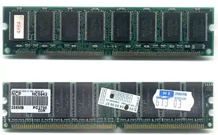
168-pin SDRAM
On the bottom edge of 168-pin DIMMs there are two notches, and the location of each notch determines a particular feature of the module. The first notch is the DRAM key position, which represents RFU (reserved future use), registered, and unbuffered DIMM types (left, middle and right position, respectively). The second notch is the voltage key position, which represents 5.0 V, 3.3 V, and RFU DIMM types (order is the same as above).
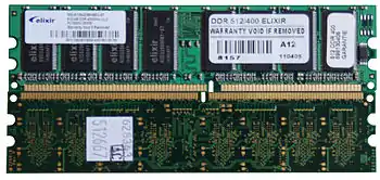
DDR DIMMs
.jpg.webp)
DDR, DDR2, DDR3, DDR4 and DDR5 all have different pin counts and/or different notch positions. As of August, 2014, DDR4 SDRAM is a modern emerging type of dynamic random access memory (DRAM) with a high-bandwidth ("double data rate") interface, and has been in use since 2013. It is the higher-speed successor to DDR, DDR2 and DDR3. DDR4 SDRAM is neither forward nor backward compatible with any earlier type of random access memory (RAM) because of different signalling voltages, timings, as well as other differing factors between the technologies and their implementation.
SPD EEPROM
A DIMM's capacity and other operational parameters may be identified with serial presence detect (SPD), an additional chip which contains information about the module type and timing for the memory controller to be configured correctly. The SPD EEPROM connects to the System Management Bus and may also contain thermal sensors (TS-on-DIMM).[2]
Error correction
ECC DIMMs are those that have extra data bits which can be used by the system memory controller to detect and correct errors. There are numerous ECC schemes, but perhaps the most common is Single Error Correct, Double Error Detect (SECDED) which uses an extra byte per 64-bit word. ECC modules usually carry a multiple of 9 instead of a multiple of 8 chips.
Ranking
Sometimes memory modules are designed with two or more independent sets of DRAM chips connected to the same address and data buses; each such set is called a rank. Ranks that share the same slot, only one rank may be accessed at any given time; it is specified by activating the corresponding rank's chip select (CS) signal. The other ranks on the module are deactivated for the duration of the operation by having their corresponding CS signals deactivated. DIMMs are currently being commonly manufactured with up to four ranks per module. Consumer DIMM vendors have recently begun to distinguish between single and dual ranked DIMMs.
After a memory word is fetched, the memory is typically inaccessible for an extended period of time while the sense amplifiers are charged for access of the next cell. By interleaving the memory (e.g. cells 0, 4, 8, etc. are stored together in one rank), sequential memory accesses can be performed more rapidly because sense amplifiers have 3 cycles of idle time for recharging, between accesses.
DIMMs are often referred to as "single-sided" or "double-sided" to describe whether the DRAM chips are located on one or both sides of the module's printed circuit board (PCB). However, these terms may cause confusion, as the physical layout of the chips does not necessarily relate to how they are logically organized or accessed.
JEDEC decided that the terms "dual-sided", "double-sided", or "dual-banked" were not correct when applied to registered DIMMs (RDIMMs).
Organization
Most DIMMs are built using "×4" ("by four") or "×8" ("by eight") memory chips with nine chips per side; "×4" and "×8" refer to the data width of the DRAM chips in bits.
In the case of "×4" registered DIMMs, the data width per side is 36 bits; therefore, the memory controller (which requires 72 bits) needs to address both sides at the same time to read or write the data it needs. In this case, the two-sided module is single-ranked. For "×8" registered DIMMs, each side is 72 bits wide, so the memory controller only addresses one side at a time (the two-sided module is dual-ranked).
The above example applies to ECC memory that stores 72 bits instead of the more common 64. There would also be one extra chip per group of eight, which is not counted.
Speeds
For various technologies, there are certain bus and device clock frequencies that are standardized; there is also a decided nomenclature for each of these speeds for each type.
DIMMs based on Single Data Rate (SDR) DRAM have the same bus frequency for data, address and control lines. DIMMs based on Double Data Rate (DDR) DRAM have data but not the strobe at double the rate of the clock; this is achieved by clocking on both the rising and falling edge of the data strobes. Power consumption and voltage gradually became lower with each generation of DDR-based DIMMs.
Another influence is Column Access Strobe (CAS) latency, or CL which affects memory access speed. This is the delay time between the READ command and the moment data is available. See main article CAS/CL
| Chip | Module | Effective Clock | Transfer rate | Voltage |
|---|---|---|---|---|
| SDR-66 | PC-66 | 66 MHz | 66 MT/s | 3.3 V |
| SDR-100 | PC-100 | 100 MHz | 100 MT/s | 3.3 V |
| SDR-133 | PC-133 | 133 MHz | 133 MT/s | 3.3 V |
| Chip | Module | Memory Clock | I/O Bus Clock | Transfer rate | Voltage |
|---|---|---|---|---|---|
| DDR-200 | PC-1600 | 100 MHz | 100 MHz | 200 MT/s | 2.5 V |
| DDR-266 | PC-2100 | 133 MHz | 133 MHz | 266 MT/s | 2.5 V |
| DDR-333 | PC-2700 | 166 MHz | 166 MHz | 333 MT/s | 2.5 V |
| DDR-400 | PC-3200 | 200 MHz | 200 MHz | 400 MT/s | 2.5 V |
| Chip | Module | Memory Clock | I/O Bus Clock | Transfer rate | Voltage |
|---|---|---|---|---|---|
| DDR2-400 | PC2-3200 | 200 MHz | 200 MHz | 400 MT/s | 1.8 V |
| DDR2-533 | PC2-4200 | 266 MHz | 266 MHz | 533 MT/s | 1.8 V |
| DDR2-667 | PC2-5300 | 333 MHz | 333 MHz | 667 MT/s | 1.8 V |
| DDR2-800 | PC2-6400 | 400 MHz | 400 MHz | 800 MT/s | 1.8 V |
| DDR2-1066 | PC2-8500 | 533 MHz | 533 MHz | 1066 MT/s | 1.8 V |
| Chip | Module | Memory Clock | I/O Bus Clock | Transfer rate | Voltage |
|---|---|---|---|---|---|
| DDR3-800 | PC3-6400 | 400 MHz | 400 MHz | 800 MT/s | 1.5 V |
| DDR3-1066 | PC3-8500 | 533 MHz | 533 MHz | 1066 MT/s | 1.5 V |
| DDR3-1333 | PC3-10600 | 667 MHz | 667 MHz | 1333 MT/s | 1.5 V |
| DDR3-1600 | PC3-12800 | 800 MHz | 800 MHz | 1600 MT/s | 1.5 V |
| DDR3-1866 | PC3-14900 | 933 MHz | 933 MHz | 1866 MT/s | 1.5 V |
| DDR3-2133 | PC3-17000 | 1066 MHz | 1066 MHz | 2133 MT/s | 1.5 V |
| DDR3-2400 | PC3-19200 | 1200 MHz | 1200 MHz | 2400 MT/s | 1.5 V |
| Chip | Module | Memory Clock | I/O Bus Clock | Transfer rate | Voltage |
|---|---|---|---|---|---|
| DDR4-1600 | PC4-12800 | 800 MHz | 800 MHz | 1600 MT/s | 1.2 V |
| DDR4-1866 | PC4-14900 | 933 MHz | 933 MHz | 1866 MT/s | 1.2 V |
| DDR4-2133 | PC4-17000 | 1066 MHz | 1066 MHz | 2133 MT/s | 1.2 V |
| DDR4-2400 | PC4-19200 | 1200 MHz | 1200 MHz | 2400 MT/s | 1.2 V |
| DDR4-2666 | PC4-21300 | 1333 MHz | 1333 MHz | 2666 MT/s | 1.2 V |
| DDR4-3200 | PC4-25600 | 1600 MHz | 1600 MHz | 3200 MT/s | 1.2 V |
Form factors
Several form factors are commonly used in DIMMs. Single Data Rate Synchronous DRAM (SDR SDRAM) DIMMs were primarily manufactured in 1.5 inches (38 mm) and 1.7 inches (43 mm) heights. When 1U rackmount servers started becoming popular, these form factor registered DIMMs had to plug into angled DIMM sockets to fit in the 1.75 inches (44 mm) high box. To alleviate this issue, the next standards of DDR DIMMs were created with a "low profile" (LP) height of around 1.2 inches (30 mm). These fit into vertical DIMM sockets for a 1U platform.
With the advent of blade servers, angled slots have once again become common in order to accommodate LP form factor DIMMs in these space-constrained boxes. This led to the development of the Very Low Profile (VLP) form factor DIMM with a height of around 0.72 inches (18 mm). The DDR3 JEDEC standard for VLP DIMM height is around 0.740 inches (18.8 mm). These will fit vertically in ATCA systems.
Full-height 240-pin DDR2 and DDR3 DIMMs are all specified at a height of around 1.18 inches (30 mm) by standards set by JEDEC. These form factors include 240-pin DIMM, SODIMM, Mini-DIMM and Micro-DIMM.[3]
Full-height 288-pin DDR4 DIMMs are slightly taller than their DDR3 counterparts at 1.23 inches (31 mm). Similarly, VLP DDR4 DIMMs are also marginally taller than their DDR3 equivalent at nearly 0.74 inches (19 mm).[4]
As of Q2 2017, Asus has had a PCI-E based "DIMM.2", which has a similar socket to DDR3 DIMMs and is used to put in a module to connect up to two M.2 NVMe solid-state drives. However, it cannot use common DDR type ram and does not have much support other than Asus.[5]
See also
- Dual in-line package (DIP)
- Memory scrambling
- Memory geometry – logical configuration of RAM modules (channels, ranks, banks, etc.)
- Motherboard
- NVDIMM – non-volatile DIMM
- Row hammer
- Rambus in-line memory module (RIMM)
- Single in-line memory module (SIMM)
- Single in-line package (SIP)
- Zig-zag in-line package (ZIP)
References
- Smith, Ryan (2020-07-14). "DDR5 Memory Specification Released: Setting the Stage for DDR5-6400 And Beyond". AnandTech. Retrieved 2020-07-15.
- Temperature Sensor in DIMM memory modules
- JEDEC MO-269J Whitepaper., accessed Aug. 20, 2014.
- JEDEC MO-309E Whitepaper., accessed Aug. 20, 2014.
- ASUS DIMM.2 is a M.2 Riser Card., accessed Jun. 4, 2020.
External links
| Wikimedia Commons has media related to DIMM. |