Physical vapor deposition
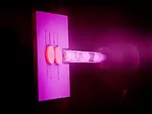
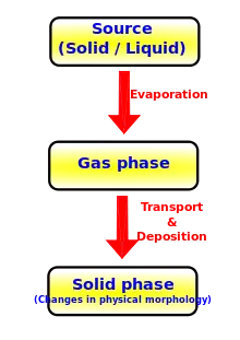
Physical vapor deposition (PVD), sometimes (especially in single-crystal growth contexts) called physical vapor transport (PVT), describes a variety of vacuum deposition methods which can be used to produce thin films and coatings. PVD is characterized by a process in which the material goes from a condensed phase to a vapor phase and then back to a thin film condensed phase. The most common PVD processes are sputtering and evaporation. PVD is used in the manufacture of items which require thin films for mechanical, optical, chemical or electronic functions. Examples include semiconductor devices such as thin film solar panels,[1] aluminized PET film for food packaging and balloons,[2] and titanium nitride coated cutting tools for metalworking. Besides PVD tools for fabrication, special smaller tools (mainly for scientific purposes) have been developed.[3]


The source material is unavoidably also deposited on most other surfaces interior to the vacuum chamber, including the fixturing used to hold the parts.
Examples
- Cathodic arc deposition: a high-power electric arc discharged at the target (source) material blasts away some into highly ionized vapor to be deposited onto the workpiece.
- Electron-beam physical vapor deposition: the material to be deposited is heated to a high vapor pressure by electron bombardment in "high" vacuum and is transported by diffusion to be deposited by condensation on the (cooler) workpiece.
- Evaporative deposition: the material to be deposited is heated to a high vapor pressure by electrical resistance heating in "high" vacuum.[4][5]
- Close-space sublimation, the material and substrate are placed close to one another and radiatively heated.
- Pulsed laser deposition: a high-power laser ablates material from the target into a vapor.
- Sputter deposition: a glow plasma discharge (usually localized around the "target" by a magnet) bombards the material sputtering some away as a vapor for subsequent deposition.
- Pulsed electron deposition: a highly energetic pulsed electron beam ablates material from the target generating a plasma stream under nonequilibrium conditions.
- Sublimation sandwich method: used for creating man-made crystals.
Various thin film characterization techniques can be used to measure the physical properties of PVD coatings, such as:
- Calo tester: coating thickness test
- Nanoindentation: hardness test for thin-film coatings
- Pin-on-disc tester: wear and friction coefficient test
- Scratch tester: coating adhesion test
- X-ray micro-analyzer: investigation of structural features and heterogeneity of elemental composition for the growth surfaces [6]
Comparison to other deposition techniques
Advantages
- PVD coatings are sometimes harder and more corrosion-resistant than coatings applied by the electroplating process. Most coatings have high temperature and good impact strength, excellent abrasion resistance and are so durable that protective topcoats are almost never necessary.
- Ability to utilize virtually any type of inorganic and some organic coating materials on an equally diverse group of substrates and surfaces using a wide variety of finishes.
- More environmentally friendly than traditional coating processes such as electroplating and painting.
- More than one technique can be used to deposit a given film.
Disadvantages
- Specific technologies can impose constraints; for example, line-of-sight transfer is typical of most PVD coating techniques, however there are methods that allow full coverage of complex geometries.
- Some PVD technologies typically operate at very high temperatures and vacuums, requiring special attention by operating personnel.
- Requires a cooling water system to dissipate large heat loads.
Applications
As mentioned previously, PVD coatings are generally used to improve hardness, wear resistance and oxidation resistance. Thus, such coatings are used in a wide range of applications such as:
- Aerospace
- Automotive
- Dies and moulds for all manner of material processing
- Cutting tools
- Firearms
- Optics
- Watches
- Jewellery
- Thin films (window tint, food packaging, etc.)
- Darts barrels
- Metals (aluminium, copper, bronze, etc.)
Decorative applications
By varying the gases and duration of process, a range of colours are produced by Physical Vapour Deposition on stainless steel. The resulting coloured stainless steel product can appear as brass, bronze and other metals or alloys. This PVD coloured stainless steel can be used as exterior cladding for buildings and structures, such as the Vessel sculpture in New York City and The Bund in Shanghai. It is also used for interior hardware, panelling and fixtures, and is even used on some consumer electronics, like the Space Gray and Gold finishes of the iPhone X, XS, and 11 Pro.
See also
References
- Selvakumar, N.; Barshilia, Harish C. (1 March 2012). "Review of physical vapor deposited (PVD) spectrally selective coatings for mid- and high-temperature solar thermal applications" (PDF). Solar Energy Materials and Solar Cells. 98: 1–23. doi:10.1016/j.solmat.2011.10.028.
- Hanlon, Joseph F.; Kelsey, Robert J.; Forcinio, Hallie (23 April 1998). "Chapter 4 Coatings and Laminations". Handbook of Package Engineering 3rd Edition. CRC Press. ISBN 978-1566763066.
- Fortunato, E.; Barquinha, P.; Martins, R. (12 June 2012). "Oxide Semiconductor Thin-Film Transistors: A Review of Recent Advances". Advanced Materials. 24 (22): 2945–2986. doi:10.1002/adma.201103228. ISSN 1521-4095. PMID 22573414.
- He, Zhenping; Kretzschmar, Ilona (6 December 2013). "Template-Assisted GLAD: Approach to Single and Multipatch Patchy Particles with Controlled Patch Shape". Langmuir. 29 (51): 15755–15761. doi:10.1021/la404592z. PMID 24313824.
- He, Zhenping; Kretzschmar, Ilona (18 June 2012). "Template-Assisted Fabrication of Patchy Particles with Uniform Patches". Langmuir. 28 (26): 9915–9919. doi:10.1021/la3017563. PMID 22708736.
- Dunaev A.A., Egorova I.L. (2015). "Properties and optical application of polycrystalline zinc selenide obtained by physical vapor deposition". Scientific and Technical Journal of Information Technologies, Mechanics and Optics. 15 (3): 449–456. doi:10.17586/2226-1494-2015-15-3-449-456.
Further reading
- Anders, André, ed. (3 October 2000). Handbook of Plasma Immersion Ion Implantation and Deposition. Wiley-VCH. ISBN 978-0471246985.
- Bach, Hans; Krause, Dieter (10 July 2003). Thin Films on Glass. Springer. ISBN 978-3540585978.
- Bunshah, Roitan F (31 December 1994). Handbook of Deposition Technologies for Films and Coatings (Second ed.). William Andrew Publishing. ISBN 978-0815517467.
- Glaser, Hans Joachim (2000). Large Area Glass Coating. Von Ardenne Anlagentechnik GMBH. ISBN 978-3000049538.
- Glocker, D; Shah, S (17 December 2001). Handbook of Thin Film Process Technology. CRC Press. ISBN 978-0750308328.
- Mahan, John E (1 February 2000). Physical Vapor Deposition of Thin Films. Wiley-Interscience. ISBN 978-0471330011.
- Mattox, Donald M. (19 May 2010). Handbook of Physical Vapor Deposition (PVD) Processing (Second ed.). William Andrew Publishing. ISBN 978-0-815-52037-5.
- Mattox, Donald M (14 January 2004). The Foundations of Vacuum Coating Technology. William Andrew Publishing. ISBN 978-0815514954.
- Mattox, Donald M.; Mattox, Vivivenne Harwood (2007). 50 Years of Vacuum Coating Technology and the Growth of the Society of Vacuum Coaters. Society of Vacuum Coaters. ISBN 978-1878068279.
- Ohring, Milton (26 October 2001). Materials Science of Thin Films, Second Edition. Academic Press. ISBN 978-1493301720.
- Powell, Carroll F.; Oxley, Joseph H.; Blocher, John Milton (1966). Klerer, J. (ed.). "Vapor Deposition". Journal of the Electrochemical Society. The Electrochemical Society. 113 (10): 226–269. ASIN B007T4PDL6. doi:10.1149/1.2423765.
- Snyder, Tim (6 May 2013). "What are PVD Wheels - Ask NASA". 4wheelonline.com. 4WheelOnline.com. Retrieved 3 October 2019.
- Westwood, William D (2003). Sputter Deposition - AVS Education Committee Book Series, Vol. 2. Education Committee, AVS. ISBN 978-0735401051.
- Willey, Ronald R (15 December 2007). Practical Monitoring and Control of Optical Thin Films. Willey Optical, Consultants. ISBN 978-0615181448.
- Willey, Ronald R (27 October 2007). Practical Equipment, Materials, and Processes for Optical Thin Films. Willey Optical, Consultants. ISBN 978-0615143972.
External links
- "Society of Vacuum Coaters". svc.org. Society of Vacuum Coaters. Retrieved 3 October 2019.
- Raghu, Saril (19 April 2009). Physical Vapor Desposition Tool. YouTube.com. Retrieved 3 October 2019.