Transition metal dichalcogenide monolayers
Transition metal dichalcogenide (TMD or TMDC) monolayers are atomically thin semiconductors of the type MX2, with M a transition metal atom (Mo, W, etc.) and X a chalcogen atom (S, Se, or Te). One layer of M atoms is sandwiched between two layers of X atoms. They are part of the large family of so-called 2D materials, named so to emphasize their extraordinary thinness. For example, a MoS2 monolayer is only 6.5 Å thick. The key feature of these materials is the interaction of large atoms in the 2D structure as compared with first-row transition metal dichalcogenides, e.g., WTe2 exhibits anomalous giant magnetoresistance and superconductivity.[1]
The discovery of graphene shows how new physical properties emerge when a bulk crystal of macroscopic dimensions is thinned down to one atomic layer. Like graphite, TMD bulk crystals are formed of monolayers bound to each other by van-der-Waals attraction. TMD monolayers have properties that are distinctly different from those of the semimetal graphene:
- TMD monolayers MoS2, WS2, MoSe2, WSe2, MoTe2 have a direct band gap, and can be used in electronics as transistors and in optics as emitters and detectors.[2][3][4][5]
- The TMD monolayer crystal structure has no inversion center, which allows to access a new degree of freedom of charge carriers, namely the k-valley index, and to open up a new field of physics: valleytronics[6][7][8][9]
- The strong spin-orbit coupling in TMD monolayers leads to a spin-orbit splitting[10] of hundreds meV in the valence band and a few meV in the conduction band, which allows control of the electron spin by tuning the excitation laser photon energy and handedness.[11]
- 2D nature and high spin-orbit coupling of MoS2 can be used as promising material for spintronic application.[12]
The work on TMD monolayers is an emerging research and development field since the discovery of the direct bandgap[2] and the potential applications in electronics [13][3] and valley physics.[7][8][9] TMDs are often combined with other 2D materials like graphene and hexagonal boron nitride to make van der Waals heterostructures. These heterostructures need to be optimized to be possibly used as building blocks for many different devices such as transistors, solar cells, LEDs, photodetectors, fuel cells, photocatalytic and sensing devices. Some of these devices are already used in everyday life and can become smaller, cheaper and more efficient by using TMD monolayers.[14][15]
Crystal structure
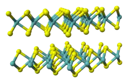
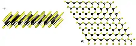
Transition metal dichalcogenides (TMDs) are composed of three atomic planes and often two atomic species: a metal and two chalcogens. The honeycomb, hexagonal lattice has three fold symmetry and can permit mirror plane symmetry and/or inversion symmetry.[16] In the macroscopic bulk crystal, or more precisely, for an even number of monolayers, the crystal structure has an inversion center. In the case of a monolayer (or any odd number of layers), the crystal may or may not have an inversion center.
Broken inversion symmetry
Two important consequences of that are:
- nonlinear optical phenomena, such as second-harmonic generation. When the crystal is excited by a laser, the output frequency can be doubled.[17][18][19][20]
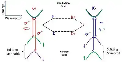
- an electronic band structure with direct energy gaps, where both conduction and valence band edges are located at the non-equivalent K points (K+ and K-) of the 2D hexagonal Brillouin zone. The interband transitions in the vicinity of the K+ (or K-) point are coupled to right (or left) circular photon polarization states. These so-called valley dependent optical selection rules arise from inversion symmetry breaking. This provides a convenient method to address specific valley states (K+ or K-) by circularly polarized (right or left) optical excitation.[9] In combination with strong spin-splitting, the spin and valley degree of freedom are coupled, enabling stable valley polarization.[21][22][23]
These properties indicate that TMD monolayers represent a promising platform to explore spin and valley physics with the corresponding possible applications.
Properties
Transport properties
At submicron scales, 3D materials no longer have the same behavior as their 2D form, which can be an advantage. For example, graphene has a very high carrier mobility, and accompanying lower losses through the Joule effect. But graphene has zero bandgap, which results in a disqualifyingly low on/off ratio in transistor applications. TMD monolayers might be an alternative: they are structurally stable, display a band gap and show electron mobilities comparable to those of silicon, so they can be used to fabricate transistors.
Although thin-layer TMDs have been found to have a lower electron mobility than bulk TMDs, most likely because their thinness makes them more susceptible to damage, it has been found that coating the TMDs with HfO2 or hexagonal boron nitride (hBN) increases their effective carrier mobility.[24]
Optical properties
| A (eV) | A (nm) | B (eV) | B (nm) | |
|---|---|---|---|---|
| MoS2 | 1.78 | 695 | 1.96 | 632 |
| MoSe2 | 1.50 | 825 | 1.75 | 708 |
| MoTe2 | 1.06 | 1170 | 1.36 | 912 |
| WS2 | 1.84 | 673 | 2.28 | 544 |
| WSe2 | 1.52 | 815 | 2.00 | 620 |
A semiconductor can absorb photons with energy larger than or equal to its bandgap. This means that light with a shorter wavelength is absorbed. Semiconductors are typically efficient emitters if the minimum of the conduction band energy is at the same position in k-space as the maximum of the valence band, i.e., the band gap is direct. The band gap of bulk TMD material down to a thickness of two monolayers is still indirect, so the emission efficiency is lower compared to monolayered materials. The emission efficiency is about 104 greater for TMD monolayer than for bulk material.[4] The band gaps of TMD monolayers are in the visible range (between 400 nm and 700 nm). The direct emission shows two excitonic transitions called A and B, separated by the spin-orbit coupling energy. The lowest energy and therefore most important in intensity is the A emission.[2][26] Owing to their direct band gap, TMD monolayers are promising materials for optoelectronics applications.
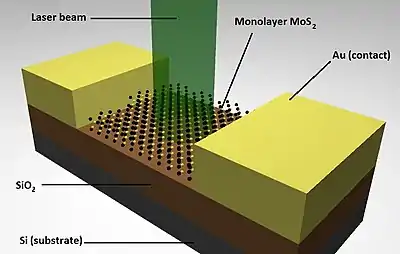
Atomic layers of MoS2 have been used as a phototransistor and ultrasensitive detectors. Phototransistors are important devices: the first with a MoS2 monolayer active region shows a photoresponsivity of 7.5 mA W−1 which is similar to graphene devices that reach 6.1 mA W−1. Multilayer MoS2 show higher photoresponsivities, about 100 mA W−1, which is similar to silicon devices. Making a gold contact at the far edges of a monolayer allows an ultrasensitive detector to be fabricated.[5] Such a detector has a photoresponsivity reaching 880 A W−1, 106 greater than the first graphene photodetectors. This high degree of electrostatic control is due to the thin active region of the monolayer. Its simplicity and the fact that it has only one semiconductor region, whereas the current generation of photodetectors is typically a p-n junction, makes possible industrial applications such as high-sensitivity and flexible photodetectors. The only limitation for currently available devices is the slow photoresponse dynamics.[5]
Mechanical properties
Interest in the use of TMD monolayers such as MoS2, WS2, and WSe2 for the use in flexible electronics due to a change from an indirect band gap in 3D to a direct band gap in 2D emphasizes the importance of the mechanical properties of these materials.[27] Unlike in bulk samples it is much more difficult to uniformly deform 2D monolayers of material and as a result, taking mechanical measurements of 2D systems is more challenging. A method that was developed to overcome this challenge, called atomic force microscopy (AFM) nanoindentation, involves bending a 2D monolayer suspended over a holey substrate with an AFM cantilever and measuring the applied force and displacement.[28] Through this method, defect free mechanically exfoliated monolayer flakes of MoS2 were found to have a Young's modulus of 270 GPa with a maximum experienced strain of 10% before breaking.[29] In the same study, it was found that bilayer mechanically exfoliated MoS2 flakes have a lower Young's modulus of 200 GPa, which is attributed to interlayer sliding and defects in the monolayer.[29] With increasing flake thickness the bending rigidity of the flake plays a dominant role and it is found that the Young's modulus of multilayer, 5- 25 layers, mechanically exfoliated MoS2 flakes is 330 GPa.[30]
The mechanical properties of other TMDs such as WS2 and WSe2 have also been determined. The Young's modulus of multilayer, 5-14 layers, mechanically exfoliated WSe2 is found to be 167 GPa with a maximum strain of 7%.[31] For WS2, the Young's modulus of chemical vapor deposited monolayer flakes is 272 GPa.[32] From this same study the Young's modulus of CVD-grown monolayer flakes of MoS2 is found to be 264 GPa.[32] This is an interesting result as the Young's modulus of the exfoliated MoS2 flake is nearly the same as that of the CVD grown MoS2 flake. It is generally accepted that chemically vapor deposited TMDs will include more defects when compared with the mechanically exfoliated films that are obtained from bulk single crystals, which implies that defects (points defects, etc.) that are included in the flake do not drastically affect the strength of the flake itself.
Under the application of strain, a decrease in the direct and indirect band gap is measured that is approximately linear with strain.[33] Importantly, the indirect bandgap decreases faster with applied strain to the monolayer than the direct bandgap, resulting in a crossover from direct to indirect band gap at a strain level of around 1%.[34] As a result, the emission efficiency of monolayers is expected to decrease for highly strained samples.[35] This property allows mechanical tuning of the electronic structure and also the possibility of fabrication of devices on flexible substrates.
Fabrication of TMD monolayers
Exfoliation
Exfoliation is a top down approach. In the bulk form, TMDs are crystals made of layers, which are coupled by Van-der-Waals forces. These interactions are weaker than the chemical bonds between the Mo and S in MoS2, for example. So TMD monolayers can be produced by micromechanical cleavage, just as graphene.
The crystal of TMD is rubbed against the surface of another material (any solid surface). In practice, adhesive tape is placed on the TMD bulk material and subsequently removed. The adhesive tape, with tiny TMD flakes coming off the bulk material, is brought down onto a substrate. On removing the adhesive tape from the substrate, TMD monolayer and multilayer flakes are deposited. This technique produces small samples of monolayer material, typically about 5–10 micrometers in diameter.[36]
Large quantities of exfoliated material can also be produced using liquid-phase exfoliation by blending TMD materials with solvents and polymers.[37]
Chemical vapor deposition
Chemical vapor deposition (CVD) is another approach used to synthesize transition metal dichalcogenides. It has been used broadly to synthesize many different TMDs because it can be easily adapted for different TMD materials. Generally, CVD growth of TMDs is achieved by putting precursors to the material, typically a transition metal oxide and pure chalcogen, into a furnace with the substrate on which the material will form.[38] The furnace is heated to high temperatures (anywhere from 650 to 1000 °C) with an inert gas, typically N2 or Ar, flowing through the tube.[38] Some materials require H2 gas as a catalyst for formation, so it may be flowed through the furnace in smaller quantities than the inert gas.[39]
Outside of traditional CVD, metal organic chemical vapor deposition (MOCVD) has been used to synthesize TMDs. Unlike traditional CVD described above, MOCVD uses gaseous precursors, as opposed to solid precursors and MOCVD is usually carried out at lower temperatures, anywhere from 300 to 900 °C.[40] MOCVD has been shown to provide more consistent wafer-scale growth than traditional CVD.
CVD is often used over mechanical exfoliation despite its added complexity because it can produce monolayers ranging anywhere from 5 to 100 microns in size as opposed to the surface areas of roughly 5-10 microns produced using the mechanical exfoliation method.[41] Not only do TMD monolayers produced by CVD have a larger surface area than those flakes produced by mechanical exfoliation, they are often more uniform. Monolayer TMD flakes with very little or no multilayer areas can be produced by chemical vapor deposition, in contrast to samples produced by mechanical exfoliation, which often have many multilayered areas.[36][38]
Molecular beam epitaxy
Molecular beam epitaxy (MBE) is an established technique for growing semiconductor devices with atomic monolayer thickness control. As a promising demonstration, high-quality monolayer MoSe2 samples have been grown on graphene by MBE.[42]
Electronic band structure
Band gap
In the bulk form, TMD have an indirect gap in the center of the Brillouin zone, whereas in monolayer form the gap becomes direct and is located in the K points.[43][2]
Spin-orbit coupling
| Valence band
splitting (eV) |
Conduction band
splitting (eV) | |
|---|---|---|
| MoS2 | 0.148 | 0.003 |
| WS2 | 0.430 | 0.026 |
| MoSe2 | 0.184 | 0.007 |
| WSe2 | 0.466 | 0.038 |
| MoTe2 | 0.219 | 0.034 |
For TMDs, the atoms are heavy and the outer layers electronic states are from d-orbitals that have a strong spin-orbit coupling. This spin orbit coupling removes the spins degeneracy in both the conduction and valence band i.e. introduces a strong energy splitting between spin up and down states. In the case of MoS2, the spin splitting in conduction band is in the meV range, it is expected to be more pronounced in other material like WS2.[46][47][48] The spin orbit splitting in the valence band is several hundred meV.
Spin-valley coupling and the electron valley degree of freedom
By controlling the charge or spin degree of freedom of carriers, as proposed by spintronics, novel devices have already been made. If there are different conduction/valence band extrema in the electronic band structure in k-space, the carrier can be confined in one of these valleys. This degree of freedom opens up a new field of physics: the controlling of carriers k-valley index, also called valleytronics.[21][49]
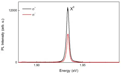
For TMD monolayers crystals, the parity symmetry is broken, there is no more inversion center. K valleys of different directions in the 2D hexagonal Brillouin zone are no longer equivalent. So there are two kinds of K valley called K+ and K-. Also there is a strong energy degeneracy of different spin states in valence band. The transformation of one valley to another is described by the time reversal operator. Moreover, crystal symmetry leads to valley dependent optical selection rules: a right circular polarized photon (σ+) initializes a carrier in the K+ valley and a left circular polarized photon (σ-) initializes a carrier in the K- valley.[7] Thanks to these two properties (spin-valley coupling and optical selection rules), a laser of specific polarization and energy allows to initialize the electron valley states (K+ or K-) and spin states (up or down).[1]
Emission and absorption of light: excitons
A single layer of TMD can absorb up to 20% of incident light,[5] which is unprecedented for such a thin material. When a photon of suitable energy is absorbed by a TMD monolayer, an electron is created in the conduction band; the electron now missing in the valence band is assimilated by a positively charged quasi-particle called a hole. The negatively charged electron and the positively charged hole are attracted via the Coulomb interaction, forming a bound state called an exciton which can be thought as a hydrogen atom (with some difference). This Bosonic-like quasi-particle is very well known and studied in traditional semiconductors, such as GaAs and ZnO but in TMD it provides exciting new opportunities for applications and for studying fundamental physics. Indeed, the reduced dielectric screening and the quantum size effect present in these ultrathin materials make the binding energy of excitons much stronger than those in traditional semiconductors. Binding energies of several hundreds of meV are observed for all the four principal members of the TMD family.[20][26][50][51][52]
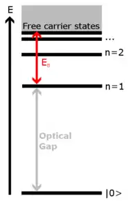
As mentioned before, we can think about an exciton as if it were a hydrogen atom, with an electron bound to a hole. The main difference is that this system is not stable and tends to relax to the vacuum state, which is here represented by an electron in the valence band. The energy difference between the exciton 'ground state' (n=1) and the 'vacuum state' is called optical gap and is the energy of the photon emitted when an exciton recombines. This is the energy of the photons emitted by TMD monolayers and observed as huge emission peaks in photoluminescence (PL) experiments, such as the one labelled X0 in the figure. In this picture the binding energy EB is defined as the difference between the free particle band gap and the optical band gap and represent, as usual, the energy needed to take the hole and the electron apart. The existence of this energy difference is called band gap renormalization. The analogy with hydrogen atom doesn't stop here as excitonic excited states were observed at higher energies and with different techniques.[20][50]
Because of the spin-orbit splitting of the valence band two different series of excitons exist in TMD, called A- and B-excitons. In the A series the hole is located in the upper branch of the Valence band while for the B-exciton the hole is in the lower branch. As a consequence the optical gap for B-exciton is larger and the corresponding peak is found at higher energy in PL and reflectivity measurements.
Another peak usually appears in the PL spectra of TMD monolayers, which is associated to different quasi-particles called trions.[54][55] These are excitons bound to another free carrier which can be either an electron or a hole. As a consequence a trion is a negative or positively charged complex. The presence of a strong trion peak in a PL spectrum, eventually stronger than the peak associated with exciton recombination, is a signature of a doped monolayer. It is believed now that this doping is extrinsic, which means that it arises from charged trap states present in the substrate (generally SiO2). Positioning a TMD monolayer between two flakes of hBN removes this extrinsic doping and greatly increase the optical quality of the sample.[53][56]
At higher excitation powers biexcitons[57][58] have also been observed in monolayer TMDs. These complexes are formed by two bound excitons. Theory predicts that even larger charge-carrier complexes, such as charged biexcitons (quintons) and ion-bound biexcitons, are stable and should be visible in the PL spectra.[59] Additionally, quantum light has been observed to originate from point defects in these materials in a variety of configurations.[60][61][62][63][64][65]
Radiation effects of TMD monolayers
Common forms of radiation used to create defects in TMDs are particle and electromagnetic irradiation, impacting the structure and electronic performance of these materials. Scientist have been studying the radiation response of these materials to be used in high-radiation environments, such as space or nuclear reactors.[66] Damage to this unique class of materials occurs mainly through sputtering and displacement for metals or radiolysis and charging for insulators and semiconductors. To sputter away an atom, the electron must be able to transfer enough energy to overcome the threshold for knock-on damage.[67] Yet, the exact quantifiable determination of this energy still needs to be determined for TMDs. Consider MoS2 as an example, TEM exposure via sputtering creates vacancies in the lattice, these vacancies are then observed to be collected together in spectroscopic lines. Additionally, when looking at the radiation response of these materials, the three parameters that are proven to matter most are the choice of substrate,[68] the sample thickness,[69] and the sample preparation process.[70]
Janus TMD monolayers
A new type of asymmetric transitional metal dichalcogenide, the Janus TMDs monolayers, has been synthesized by breaking the out-of-plane structural symmetry via plasma assisted chemical vapor deposition.[71] Janus TMDs monolayers show an asymmetric structure MXY (M = Mo or W, X/Y = S, Se or Te)[72] exhibiting out-of-plane optical dipole[73] and piezoelectricity[74] due to the imbalance of the electronic wave-function between the dichalcogenides, which are absent in a non-polar TMDs monolayer, MX2. In addition, the asymmetric structure of Janus MoSSe provides an enhanced Rashba spin-orbit interaction, which suggests asymmetrically Janus TMDs monolayer can be a promising candidate for spintronic applications. In addition, Janus TMDs monolayer has been considered as an excellent material for electrocatalysis[75] or photocatalysis.[76]
Janus MoSSe can be synthesized by inductively coupled plasma CVD (ICP-CVD). The top layer of sulfur atoms on MoS2 is stripped using hydrogen ions, forming an intermediate state, MoSH. Afterward, the intermediate state is selenized by thermal annealing at 250 °C in an environment of hydrogen and argon gases.[71]
Applications
Electronics
In 2011, the first field-effect transistor (FET) made of monolayer MoS2 was reported. It showed an excellent on/off ratio exceeding 108 at room temperature owing to excellent electrostatic control over the conduction in the 2D channel.[77] Following this, FETs made from MoS2, MoSe2, WS2, and WSe2 have been made. All show promise not just because of their electron mobility and band gap, but because their very thin structure makes them promising for use in thin, flexible electronics.[78]
Sensing
The band gap TMDs possess makes them ideal for atomically thin sensors as a replacement for graphene. These sensors have been used to sense anything from gases to liquids to biological materials like proteins or DNA. Most often, the sensors are based upon FETs, which I will elaborate upon above. FET-based biosensors rely on receptors attached to the monolayer TMD. When target molecules attach to the receptors, it affects the current flowing through the transistor.[79]
However, it has been shown that one can detect nitrogenous bases in DNA when they pass through nanopores made in MoS2.[80] Nanopore sensors are based upon measuring ionic current through a nanopore in a material. When a single strand of DNA passes through the pore, there is a marked decrease in ionic current for each base. By measuring the current flowing through the nanopore, the DNA can then be sequenced.[80]
To this date, most sensors have been created from MoS2, although WS2 has been explored as a potential sensor.[81]
References
- Eftekhari, A. (2017). "Tungsten dichalcogenides (WS2, WSe2, and WTe2): materials chemistry and applications". Journal of Materials Chemistry A. 5 (35): 18299–18325. doi:10.1039/C7TA04268J.
- Splendiani, A.; Sun, L.; Zhang, Y.; Li, T.; Kim, J.; Chim, C. Y.; Galli, G.; Wang, F. (2010). "Emerging Photoluminescence in Monolayer MoS2". Nano Letters. 10 (4): 1271–5. Bibcode:2010NanoL..10.1271S. doi:10.1021/nl903868w. PMID 20229981.
- Radisavljevic, B.; Radenovic, A.; Brivio, J.; Giacometti, V.; Kis, A. (2011). "Single-layer MoS2 transistors". Nature Nanotechnology. 6 (3): 147–50. Bibcode:2011NatNa...6..147R. doi:10.1038/nnano.2010.279. PMID 21278752.
- Sundaram, R. S.; Engel, M.; Lombardo, A.; Krupke, R.; Ferrari, A. C.; Avouris, Ph; Steiner, M. (2013). "Electroluminescence in Single Layer MoS2". Nano Letters. 13 (4): 1416–1421. arXiv:1211.4311. Bibcode:2013NanoL..13.1416S. doi:10.1021/nl400516a. PMID 23514373. S2CID 207581247.
- Lopez-Sanchez, O.; Lembke, D.; Kayci, M.; Radenovic, A.; Kis, A. (2013). "Ultrasensitive photodetectors based on monolayer MoS2". Nature Nanotechnology. 8 (7): 497–501. Bibcode:2013NatNa...8..497L. doi:10.1038/nnano.2013.100. PMID 23748194.
- Rycerz, A.; Tworzydło, J.; Beenakker, C. W. J. (2007). "Valley filter and valley valve in graphene". Nature Physics. 3 (3): 172–175. arXiv:cond-mat/0608533. Bibcode:2007NatPh...3..172R. doi:10.1038/nphys547. S2CID 119377206.
- Cao, T.; Wang, G.; Han, W.; Ye, H.; Zhu, C.; Shi, J.; Niu, Q.; Tan, P.; Wang, E.; Liu, B.; Feng, J. (2012). "Valley-selective circular dichroism of monolayer molybdenum disulphide". Nature Communications. 3 (6): 887. arXiv:1112.4013. Bibcode:2012NatCo...3E.887C. doi:10.1038/ncomms1882. PMC 3621397. PMID 22673914.
- Mak, K. F.; He, K.; Shan, J.; Heinz, T. F. (2012). "Control of valley polarization in monolayer MoS2 by optical helicity". Nature Nanotechnology. 7 (8): 494–8. arXiv:1205.1822. Bibcode:2012NatNa...7..494M. doi:10.1038/nnano.2012.96. PMID 22706698. S2CID 23248686.
- Zeng, H.; Dai, J.; Yao, W.; Xiao, D.; Cui, X. (2012). "Valley polarization in MoS2 monolayers by optical pumping". Nature Nanotechnology. 7 (8): 490–3. arXiv:1202.1592. Bibcode:2012NatNa...7..490Z. doi:10.1038/nnano.2012.95. PMID 22706701. S2CID 13228054.
- Reyes-Retana, J.A.; Cervantes-Sodi, F. (2016). "Spin-orbital effects in metal-dichalcogenide semiconducting monolayers". Scientific Reports. 6: 24093. Bibcode:2016NatSR...624093R. doi:10.1038/srep24093. PMC 4837337. PMID 27094967.
- Sallen, G.; Bouet, L.; Marie, X.; Wang, G.; Zhu, C.R.; Han, W.P.; Lu, P.; Tan, P.H.; Amand, T; Liu, B.L.; Urbaszek, B. (2012). "Robust optical emission polarization in MoS2 monolayers through selective valley excitation". Physical Review B. 86 (8): 3–6. arXiv:1206.5128. Bibcode:2012PhRvB..86h1301S. doi:10.1103/PhysRevB.86.081301. S2CID 62890713.
- Husain, Sajid; Kumar, Abhishek; Kumar, Prabhat; Kumar, Ankit; Barwal, Vineet; Behera, Nilamani; Choudhary, Sudhanshu; Svedlindh, Peter; Chaudhary, Sujeet (2018). "Spin pumping in the Heusler alloy Co2FeAl/MoS2 heterostructure: Ferromagnetic resonance experiment and theory". Physical Review B. 98 (18): 180404. Bibcode:2018PhRvB..98r0404H. doi:10.1103/PhysRevB.98.180404.
- Briggs, Natalie; Subramanian, Shruti; Lin, Zhong; Li, Xufan; Zhang, Xiaotian; Zhang, Kehao; Xiao, Kai; Geohegan, David; Wallace, Robert; Chen, Long-Qing; Terrones, Mauricio; Ebrahimi, Aida; Das, Saptarshi; Redwing, Joan; Hinkle, Christopher; Momeni, Kasra; van Duin, Adri; Crespi, Vin; Kar, Swastik; Robinson, Joshua A. (2019). "A roadmap for electronic grade 2D materials". 2D Materials. 6 (2): 022001. Bibcode:2019TDM.....6b2001B. doi:10.1088/2053-1583/aaf836. OSTI 1503991.
- "2-D materials enhance a 3-D world". phys.org. 2017-01-10.
- Nealon, Cory (2016-05-13). "This 'nanocavity' may improve ultrathin solar panels, video cameras and more". phys.org.
- Sung, S.H.; Schnitzer, N.; Brown, L.; Park, J.; Hovden, R. (2019). "Stacking, strain, and twist in 2D materials quantified by 3D electron diffraction". Physical Review Materials. 3 (6): 064003. arXiv:1905.11354. Bibcode:2019PhRvM...3f4003S. doi:10.1103/PhysRevMaterials.3.064003. S2CID 166228311.
- Kumar, N.; Najmaei, S.; Cui, Q.; Ceballos, F.; Ajayan, P.; Lou, J.; Zhao, H. (2013). "Second harmonic microscopy of monolayer MoS2". Physical Review B. 87 (16): 161403. arXiv:1302.3935. Bibcode:2013PhRvB..87p1403K. doi:10.1103/PhysRevB.87.161403. S2CID 1796583.
- Malard, L. M.; Alencar, T. V.; Barboza, A. P. M.; Mak, K. F.; De Paula, A. M. (2013). "Observation of intense second harmonic generation from MoS2 atomic crystals". Physical Review B. 87 (20): 201401. arXiv:1304.4289. Bibcode:2013PhRvB..87t1401M. doi:10.1103/PhysRevB.87.201401. S2CID 118392637.
- Zeng, H.; Liu, G. B.; Dai, J.; Yan, Y.; Zhu, B.; He, R.; Xie, L.; Xu, S.; Chen, X.; Yao, W.; Cui, X. (2013). "Optical signature of symmetry variations and spin-valley coupling in atomically thin tungsten dichalcogenides". Scientific Reports. 3: 1608. arXiv:1208.5864. Bibcode:2013NatSR...3E1608Z. doi:10.1038/srep01608. PMC 3622914. PMID 23575911.
- Wang, G.; Marie, X.; Gerber, I.; Amand, T.; Lagarde, D.; Bouet, L.; Vidal, M.; Balocchi, A.; Urbaszek, B. (2015). "Giant Enhancement of the Optical Second-Harmonic Emission of WSe2 Monolayers by Laser Excitation at Exciton Resonances". Physical Review Letters. 114 (9): 097403. arXiv:1404.0056. Bibcode:2015PhRvL.114i7403W. doi:10.1103/PhysRevLett.114.097403. PMID 25793850.
- Xiao, D.; Liu, G. B.; Feng, W.; Xu, X.; Yao, W. (2012). "Coupled Spin and Valley Physics in Monolayers of MoS2 and Other Group-VI Dichalcogenides". Physical Review Letters. 108 (19): 196802. arXiv:1112.3144. Bibcode:2012PhRvL.108s6802X. doi:10.1103/PhysRevLett.108.196802. PMID 23003071. S2CID 13621082.
- Jones, A. M.; Yu, H.; Ghimire, N. J.; Wu, S.; Aivazian, G.; Ross, J. S.; Zhao, B.; Yan, J.; Mandrus, D. G.; Xiao, D.; Yao, W.; Xu, X. (2013). "Optical generation of excitonic valley coherence in monolayer WSe2". Nature Nanotechnology. 8 (9): 634–8. arXiv:1303.5318. Bibcode:2013NatNa...8..634J. doi:10.1038/nnano.2013.151. PMID 23934096. S2CID 7090218.
- Xu, X.; Yao, W.; Xiao, D.; Heinz, T. F. (2014). "Spin and pseudospins in layered transition metal dichalcogenides". Nature Physics. 10 (5): 343–350. Bibcode:2014NatPh..10..343X. doi:10.1038/nphys2942.
- Manzeli, Sajedeh; Ovchinnikov, Dmitry; Pasquier, Diego; Yazyev, Oleg V.; Kis, Andras (2017-06-13). "2D transition metal dichalcogenides". Nature Reviews Materials. 2 (8): 1–15. doi:10.1038/natrevmats.2017.33. ISSN 2058-8437.
- Ramasubramaniam, A. (2012). "Large excitonic effects in monolayers of molybdenum and tungsten dichalcogenides". Physical Review B. 86 (11): 115409. Bibcode:2012PhRvB..86k5409R. doi:10.1103/PhysRevB.86.115409.
- Qiu, D. Y.; Da Jornada, F. H.; Louie, S. G. (2013). "Optical Spectrum of MoS2: Many-Body Effects and Diversity of Exciton States". Physical Review Letters. 111 (21): 216805. arXiv:1311.0963. Bibcode:2013PhRvL.111u6805Q. doi:10.1103/PhysRevLett.111.216805. PMID 24313514. S2CID 19063715.
- Akinwande, Deji; Petrone, Nicholas; Hone, James (2014-12-17). "Two-dimensional flexible nanoelectronics". Nature Communications. 5: 5678. Bibcode:2014NatCo...5.5678A. doi:10.1038/ncomms6678. PMID 25517105.
- Lee, Changgu; Wei, Xiaoding; Kysar, Jeffrey W.; Hone, James (2008-07-18). "Measurement of the Elastic Properties and Intrinsic Strength of Monolayer Graphene". Science. 321 (5887): 385–388. Bibcode:2008Sci...321..385L. doi:10.1126/science.1157996. PMID 18635798. S2CID 206512830.
- Bertolazzi, Simone; Brivio, Jacopo; Kis, Andras (2011-11-16). "Stretching and Breaking of Ultrathin MoS2". ACS Nano. 5 (12): 9703–9709. doi:10.1021/nn203879f. PMID 22087740.
- Castellanos-Gomez, Andres; Poot, Menno; Steele, Gary A.; van der Zant, Herre S. J.; Agraït, Nicolás; Rubio-Bollinger, Gabino (2012). "Elastic Properties of Freely Suspended MoS2 Nanosheets". Advanced Materials. 24 (6): 772–775. arXiv:1202.4439. Bibcode:2012arXiv1202.4439C. doi:10.1002/adma.201103965. PMID 22231284. S2CID 205243099.
- Zhang, Rui; Koutsos, Vasileious; Cheung, Cheung (January 2016). "Elastic properties of suspended multilayer WSe2". Applied Physics Letters. 108 (4): 042104. Bibcode:2016ApPhL.108d2104Z. doi:10.1063/1.4940982.
- Liu, Kai; Yan, Qimin; Chen, Michelle; Fan, Wen; Sun, Yinghui; Suh, Joonki; Fu, Deyi; Lee, Sangwook; Zhou, Jian (2014). "Elastic Properties of Chemical-Vapor-Deposited Monolayer MoS2, WS2, and Their Bilayer Heterostructures". Nano Letters. 14 (9): 5097–5103. arXiv:1407.2669. Bibcode:2014NanoL..14.5097L. doi:10.1021/nl501793a. PMID 25120033. S2CID 2136100.
- He, K.; Poole, C.; Mak, K. F.; Shan, J. (2013). "Experimental Demonstration of Continuous Electronic Structure Tuning via Strain in Atomically Thin MoS2". Nano Letters. 13 (6): 2931–6. arXiv:1305.3673. Bibcode:2013NanoL..13.2931H. doi:10.1021/nl4013166. PMID 23675872. S2CID 207691793.
- Conley, H. J.; Wang, B.; Ziegler, J. I.; Haglund, R. F.; Pantelides, S. T.; Bolotin, K. I. (2013). "Bandgap Engineering of Strained Monolayer and Bilayer MoS2". Nano Letters. 13 (8): 3626–30. arXiv:1305.3880. Bibcode:2013NanoL..13.3626C. doi:10.1021/nl4014748. PMID 23819588. S2CID 8191142.
- Zhu, C. R.; Wang, G.; Liu, B. L.; Marie, X.; Qiao, X. F.; Zhang, X.; Wu, X. X.; Fan, H.; Tan, P. H.; Amand, T.; Urbaszek, B. (2013). "Strain tuning of optical emission energy and polarization in monolayer and bilayer MoS2". Physical Review B. 88 (12): 121301. arXiv:1306.3442. Bibcode:2013PhRvB..88l1301Z. doi:10.1103/PhysRevB.88.121301. S2CID 119269184.
- Novoselov, K. S.; Jiang, D; Schedin, F; Booth, T. J.; Khotkevich, V. V.; Morozov, S. V.; Geim, A. K. (2005). "Two-dimensional atomic crystals". Proceedings of the National Academy of Sciences. 102 (30): 10451–3. arXiv:cond-mat/0503533. Bibcode:2005PNAS..10210451N. doi:10.1073/pnas.0502848102. PMC 1180777. PMID 16027370.
- Coleman, Jonathan N.; Lotya, Mustafa; O’Neill, Arlene; Bergin, Shane D.; King, Paul J.; Khan, Umar; Young, Karen; Gaucher, Alexandre; De, Sukanta; Smith, Ronan J.; Shvets, Igor V.; Arora, Sunil K.; Stanton, George; Kim, Hye-Young; Lee, Kangho; Kim, Gyu Tae; Duesberg, Georg S.; Hallam, Toby; Boland, John J.; Wang, Jing Jing; Donegan, John F.; Grunlan, Jaime C.; Moriarty, Gregory; Shmeliov, Aleksey; Nicholls, Rebecca J.; Perkins, James M.; Grieveson, Eleanor M.; Theuwissen, Koenraad; McComb, David W.; Nellist, Peter D.; Nicolosi, Valeria (2011). "Two-Dimensional Nanosheets Produced by Liquid Exfoliation of Layered Materials". Science. 331 (6017): 568–571. Bibcode:2011Sci...331..568C. doi:10.1126/science.1194975. hdl:2262/66458. PMID 21292974. S2CID 23576676.
- Kim, Se‐Yang; Kwak, Jinsung; Ciobanu, Cristian V.; Kwon, Soon‐Yong (February 2019). "Recent Developments in Controlled Vapor‐Phase Growth of 2D Group 6 Transition Metal Dichalcogenides". Advanced Materials. 31 (20): 1804939. doi:10.1002/adma.201804939. ISSN 0935-9648. PMID 30706541.
- Shi, Yumeng; Li, Henan; Li, Lain-Jong (2015-04-28). "Recent advances in controlled synthesis of two-dimensional transition metal dichalcogenides via vapour deposition techniques". Chemical Society Reviews. 44 (9): 2744–2756. doi:10.1039/C4CS00256C. ISSN 1460-4744. PMID 25327436.
- "AIXTRON Technologies: MOCVD :: AIXTRON". www.aixtron.com. Retrieved 2019-12-02.
- Lee, Y. H.; Zhang, X. Q.; Zhang, W; Chang, M. T.; Lin, C. T.; Chang, K. D.; Yu, Y. C.; Wang, J. T.; Chang, C. S.; Li, L. J.; Lin, T. W. (2012). "Synthesis of large-area MoS2 atomic layers with chemical vapor deposition". Advanced Materials. 24 (17): 2320–5. arXiv:1202.5458. Bibcode:2012arXiv1202.5458L. doi:10.1002/adma.201104798. PMID 22467187. S2CID 11713759.
- Zhang, Y.; Chang, T. R.; Zhou, B.; Cui, Y. T.; Yan, H.; Liu, Z.; Schmitt, F.; Lee, J.; Moore, R.; Chen, Y.; Lin, H.; Jeng, H. T.; Mo, S. K.; Hussain, Z.; Bansil, A.; Shen, Z. X. (2013). "Direct observation of the transition from indirect to direct bandgap in atomically thin epitaxial MoSe2". Nature Nanotechnology. 9 (2): 111–5. arXiv:1401.3386. Bibcode:2014NatNa...9..111Z. doi:10.1038/nnano.2013.277. PMID 24362235. S2CID 19888413.
- Mak, K. F.; Lee, C.; Hone, J.; Shan, J.; Heinz, T. F. (2010). "Atomically Thin MoS2: A New Direct-Gap Semiconductor". Physical Review Letters. 105 (13): 136805. arXiv:1004.0546. Bibcode:2010PhRvL.105m6805M. doi:10.1103/PhysRevLett.105.136805. PMID 21230799. S2CID 40589037.
- Cheng, Y. C.; Zhu, Z. Y.; Tahir, M.; Schwingenschlogl, U. (2012). "Spin-orbit–induced spin splittings in polar transition metal dichalcogenide monolayers". EPL. 102 (5): 57001. Bibcode:2013EL....10257001C. doi:10.1209/0295-5075/102/57001.
- Liu, G. B.; Shan, W. Y.; Yao, Y.; Yao, W.; Xiao, D. (2013). "Three-band tight-binding model for monolayers of group-VIB transition metal dichalcogenides". Physical Review B. 88 (8): 085433. arXiv:1305.6089. Bibcode:2013PhRvB..88h5433L. doi:10.1103/PhysRevB.88.085433. S2CID 119111681.
- Zhu, Z.; Cheng, Y. C.; Schwingenschlogl, U. (2011). "Giant spin-orbit-induced spin splitting in two-dimensional transition-metal dichalcogenide semiconductors". Physical Review B. 84 (15): 153402. Bibcode:2011PhRvB..84o3402Z. doi:10.1103/PhysRevB.84.153402. hdl:10754/315771.
- Kośmider, K.; González, J. W.; Fernández-Rossier, J. (2013). "Large spin splitting in the conduction band of transition metal dichalcogenide monolayers". Physical Review B. 88 (24): 245436. arXiv:1311.0049. Bibcode:2013PhRvB..88x5436K. doi:10.1103/PhysRevB.88.245436. S2CID 31176688.
- Kormányos, A.; Zólyomi, V.; Drummond, N. D.; Burkard, G. (2014). "Spin-Orbit Coupling, Quantum Dots, and Qubits in Monolayer Transition Metal Dichalcogenides". Physical Review X. 4 (1): 011034. arXiv:1310.7720. Bibcode:2014PhRvX...4a1034K. doi:10.1103/PhysRevX.4.011034. S2CID 17909293.
- Bussolotti, Fabio; Kawai, Hiroyo; Ooi, Zi En; Chellappan, Vijila; Thian, Dickson; Pang, Ai Lin Christina; Goh, Kuan Eng Johnson (2018). "Roadmap on finding chiral valleys: screening 2D materials for valleytronics". Nano Futures. 2 (3): 032001. Bibcode:2018NanoF...2c2001B. doi:10.1088/2399-1984/aac9d7.
- Chernikov, Alexey; Berkelbach, Timothy C.; Hill, Heather M.; Rigosi, Albert; Li, Yilei; Aslan, Ozgur Burak; Reichman, David R.; Hybertsen, Mark S.; Heinz, Tony F. (2014). "Exciton Binding Energy and Nonhydrogenic Rydberg Series in Monolayer WS2". Physical Review Letters. 113 (7): 076802. arXiv:1403.4270. Bibcode:2014PhRvL.113g6802C. doi:10.1103/PhysRevLett.113.076802. PMID 25170725. S2CID 23157872.
- Ye, Ziliang; Cao, Ting; O’Brien, Kevin; Zhu, Hanyu; Yin, Xiaobo; Wang, Yuan; Louie, Steven G.; Zhang, Xiang (2014). "Probing excitonic dark states in single-layer tungsten disulphide". Nature. 513 (7517): 214–218. arXiv:1403.5568. Bibcode:2014Natur.513..214Y. doi:10.1038/nature13734. PMID 25162523. S2CID 4461357.
- Ugeda, M. M.; Bradley, A. J.; Shi, S. F.; Da Jornada, F. H.; Zhang, Y.; Qiu, D. Y.; Ruan, W.; Mo, S. K.; Hussain, Z.; Shen, Z. X.; Wang, F.; Louie, S. G.; Crommie, M. F. (2014). "Giant bandgap renormalization and excitonic effects in a monolayer transition metal dichalcogenide semiconductor". Nature Materials. 13 (12): 1091–1095. arXiv:1404.2331. Bibcode:2014NatMa..13.1091U. doi:10.1038/nmat4061. PMID 25173579. S2CID 25491405.
- Manca, M.; Glazov, M. M.; Robert, C.; Cadiz, F.; Taniguchi, T.; Watanabe, K.; Courtade, E.; Amand, T.; Renucci, P.; Marie, X.; Wang, G.; Urbaszek, B. (2017). "Enabling valley selective exciton scattering in monolayer WSe2 through upconversion". Nat. Commun. 8: 14927. arXiv:1701.05800. Bibcode:2017NatCo...814927M. doi:10.1038/ncomms14927. PMC 5382264. PMID 28367962.
- Ross, J. S.; et al. (2013). "Electrical control of neutral and charged excitons in a monolayer semiconductor". Nat. Commun. 4: 1474. arXiv:1211.0072. Bibcode:2013NatCo...4.1474R. doi:10.1038/ncomms2498. PMID 23403575. S2CID 9872370.
- Mak, K. F.; et al. (2013). "Tightly bound trions in monolayer MoS2". Nat. Mater. 12 (3): 207–211. arXiv:1210.8226. Bibcode:2013NatMa..12..207M. doi:10.1038/nmat3505. PMID 23202371. S2CID 205408065.
- Cadiz, F.; Courtade, E.; Robert, C.; Wang, G.; Shen, Y.; Cai, H.; Taniguchi, T.; Watanabe, K.; Carrere, H.; Lagarde, D.; Manca, M.; Amand, T.; Renucci, P.; Tongay, S.; Marie, X.; Urbaszek, B. (2017). "Excitonic linewidth approaching the homogeneous limit in MoS2 based van der Waals heterostructures : accessing spin-valley dynamics". Physical Review X. 7 (2): 021026. arXiv:1702.00323. Bibcode:2017PhRvX...7b1026C. doi:10.1103/PhysRevX.7.021026. S2CID 55508192.
- Mai, C.; et al. (2014). "Many-Body Effects in Valleytronics: Direct Measurement of Valley Lifetimes in Single-Layer MoS2". Nano Lett. 14 (1): 202–206. Bibcode:2014NanoL..14..202M. doi:10.1021/nl403742j. PMID 24325650.
- Shang, J.; et al. (2015). "Observation of Excitonic Fine Structure in a 2D Transition-Metal Dichalcogenide Semiconductor". ACS Nano. 9 (1): 647–655. doi:10.1021/nn5059908. PMID 25560634.
- Mostaani, E.; et al. (2017). "Diffusion quantum Monte Carlo study of excitonic complexes in two-dimensional transition-metal dichalcogenides". Physical Review B. 96 (7): 075431. arXiv:1706.04688. Bibcode:2017PhRvB..96g5431M. doi:10.1103/PhysRevB.96.075431. S2CID 46144082.
- Kern, Johannes; Niehues, Iris; Tonndorf, Philipp; Schmidt, Robert; Wigger, Daniel; Schneider, Robert; Stiehm, Torsten; Michaelis de Vasconcellos, Steffen; Reiter, Doris E. (September 2016). "Nanoscale Positioning of Single-Photon Emitters in Atomically Thin WSe2". Advanced Materials. 28 (33): 7101–7105. doi:10.1002/adma.201600560. PMID 27305430.
- He, Yu-Ming; Clark, Genevieve; Schaibley, John R.; He, Yu; Chen, Ming-Cheng; Wei, Yu-Jia; Ding, Xing; Zhang, Qiang; Yao, Wang (2015). "Single quantum emitters in monolayer semiconductors". Nature Nanotechnology. 10 (6): 497–502. arXiv:1411.2449. Bibcode:2015NatNa..10..497H. doi:10.1038/nnano.2015.75. PMID 25938571. S2CID 205454184.
- Palacios-Berraquero, Carmen; Kara, Dhiren M.; Montblanch, Alejandro R.-P.; Barbone, Matteo; Latawiec, Pawel; Yoon, Duhee; Ott, Anna K.; Loncar, Marko; Ferrari, Andrea C. (August 2017). "Large-scale quantum-emitter arrays in atomically thin semiconductors". Nature Communications. 8 (1): 15093. arXiv:1609.04244. Bibcode:2017NatCo...815093P. doi:10.1038/ncomms15093. PMC 5458119. PMID 28530249.
- Palacios-Berraquero, Carmen; Barbone, Matteo; Kara, Dhiren M.; Chen, Xiaolong; Goykhman, Ilya; Yoon, Duhee; Ott, Anna K.; Beitner, Jan; Watanabe, Kenji (December 2016). "Atomically thin quantum light-emitting diodes". Nature Communications. 7 (1): 12978. arXiv:1603.08795. Bibcode:2016NatCo...712978P. doi:10.1038/ncomms12978. PMC 5052681. PMID 27667022.
- Wu, Wei; Dass, Chandriker K.; Hendrickson, Joshua R.; Montaño, Raul D.; Fischer, Robert E.; Zhang, Xiaotian; Choudhury, Tanushree H.; Redwing, Joan M.; Wang, Yongqiang (2019). "Locally defined quantum emission from epitaxial few-layer tungsten diselenide". Applied Physics Letters. 114 (21): 213102. Bibcode:2019ApPhL.114u3102W. doi:10.1063/1.5091779.
- Dass, Chandriker Kavir; Khan, Mahtab A.; Clark, Genevieve; Simon, Jeffrey A.; Gibson, Ricky; Mou, Shin; Xu, Xiaodong; Leuenberger, Michael N.; Hendrickson, Joshua R. (2019). "Ultra‐Long Lifetimes of Single Quantum Emitters in Monolayer WSe2/hBN Heterostructures". Advanced Quantum Technologies. 2 (5–6): 1900022. doi:10.1002/qute.201900022.
- Srour, J.R.; McGarity, J.M. (1988). "Radiation effects on microelectronics in space". Proc. IEEE. 76 (11): 1443–1469. doi:10.1109/5.90114.
- Walker, R.C.; Shi, T. (2016). "Radiation effects on two-dimensional materials". Proc. Physical Status Solida.
- Freitag, M.; Low, T.; Avouris, P. (2013). "Increased responsivity of suspended graphene photodetectors". Nano Letters. 13 (4): 1644–1648. Bibcode:2013NanoL..13.1644F. doi:10.1021/nl4001037. PMID 23452264.
- Lee, H.S. (2012). "MoS2 nanosheet phototransistors with thickness-modulated optical energy gap". Nano Letters. 12 (7): 3695–3700. doi:10.1021/nl301485q. PMID 22681413.
- Liu, F.; Shimotani, H.; Shang, H. (2014). "High-sensitivity photodetectors based on multilayer GaTe flakes". ACS Nano. 8 (1): 752–760. doi:10.1021/nn4054039. PMID 24364508.
- Lu, Ang-Yu; Zhu, Hanyu; Xiao, Jun; Chuu, Chih-Piao; Han, Yimo; Chiu, Ming-Hui; Cheng, Chia-Chin; Yang, Chih-Wen; Wei, Kung-Hwa; Yang, Yiming; Wang, Yuan; Sokaras, Dimosthenis; Nordlund, Dennis; Yang, Peidong; Muller, David A.; Chou, Mei-Yin; Zhang, Xiang; Li, Lain-Jong (2017). "Janus monolayers of transition metal dichalcogenides". Nature Nanotechnology. 12 (8): 744–749. doi:10.1038/nnano.2017.100. PMID 28507333.
- Cheng, Y. C.; Zhu, Z. Y.; Tahir, M.; Schwingenschlögl, U. (2013). "Spin-orbit–induced spin splittings in polar transition metal dichalcogenide monolayers". EPL (Europhysics Letters). 102 (5): 57001. Bibcode:2013EL....10257001C. doi:10.1209/0295-5075/102/57001.
- Li, Fengping; Wei, Wei; Zhao, Pei; Huang, Baibiao; Dai, Ying (2017). "Electronic and Optical Properties of Pristine and Vertical and Lateral Heterostructures of Janus MoSSe and WSSe". The Journal of Physical Chemistry Letters. 8 (23): 5959–5965. doi:10.1021/acs.jpclett.7b02841. PMID 29169238.
- Dong, Liang; Lou, Jun; Shenoy, Vivek B. (2017). "Large In-Plane and Vertical Piezoelectricity in Janus Transition Metal Dichalchogenides". ACS Nano. 11 (8): 8242–8248. doi:10.1021/acsnano.7b03313. PMID 28700210.
- Zhang, Jing; Jia, Shuai; Kholmanov, Iskandar; Dong, Liang; Er, Dequan; Chen, Weibing; Guo, Hua; Jin, Zehua; Shenoy, Vivek B. (2017). "Janus Monolayer Transition-Metal Dichalcogenides". ACS Nano. 11 (8): 8192–8198. arXiv:1704.06389. doi:10.1021/acsnano.7b03186. PMID 28771310. S2CID 31445401.
- Ma, Xiangchao; Wu, Xin; Wang, Haoda; Wang, Yucheng (2018). "A Janus MoSSe monolayer: a potential wide solar-spectrum water-splitting photocatalyst with a low carrier recombination rate". Journal of Materials Chemistry A. 6 (5): 2295–2301. doi:10.1039/c7ta10015a.
- Radisavljevic, B.; Radenovic, A.; Brivio, J.; Giacometti, V.; Kis, A. (2011). "Single-layer MoS2 transistors". Nature Nanotechnology. 6 (3): 147–50. Bibcode:2011NatNa...6..147R. doi:10.1038/nnano.2010.279. PMID 21278752.
- Choi, Wonbong; Choudhary, Nitin; Han, Gang Hee; Park, Juhong; Akinwande, Deji; Lee, Young Hee (2017-04-01). "Recent development of two-dimensional transition metal dichalcogenides and their applications". Materials Today. 20 (3): 116–130. doi:10.1016/j.mattod.2016.10.002. ISSN 1369-7021.
- Syu, Yu-Cheng; Hsu, Wei-En; Lin, Chih-Ting (2018-01-01). "Review—Field-Effect Transistor Biosensing: Devices and Clinical Applications". ECS Journal of Solid State Science and Technology. 7 (7): Q3196–Q3207. doi:10.1149/2.0291807jss. ISSN 2162-8769.
- Barua, Shaswat; Dutta, Hemant Sankar; Gogoi, Satyabrat; Devi, Rashmita; Khan, Raju (2018-01-26). "Nanostructured MoS2-Based Advanced Biosensors: A Review". ACS Applied Nano Materials. 1 (1): 2–25. doi:10.1021/acsanm.7b00157.
- Hu, Yanling; Huang, Ying; Tan, Chaoliang; Zhang, Xiao; Lu, Qipeng; Sindoro, Melinda; Huang, Xiao; Huang, Wei; Wang, Lianhui; Zhang, Hua (2016-11-30). "Two-dimensional transition metal dichalcogenide nanomaterials for biosensing applications". Materials Chemistry Frontiers. 1 (1): 24–36. doi:10.1039/C6QM00195E. ISSN 2052-1537.