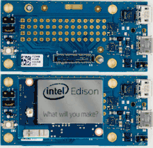
Intel Edison
The Intel Edison is a computer-on-module that was offered by Intel as a development system for wearable devices[2] and Internet of Things devices. The system was initially announced to be the same size and shape as an SD card and containing a dual-core Intel Quark x86[3] CPU at 400 MHz communicating via Bluetooth and Wi-Fi.[4][5] A later announcement changed the CPU to a 500 MHz Silvermont dual-core Intel Atom CPU,[6] and in September 2014 a second version of Edison was shown at IDF, which was bigger and thicker than a standard SD card.[7][8][9]
 | |
| Developer | Intel Corporation |
|---|---|
| Type | Tiny Board Computer |
| Release date | Q3'14 |
| Discontinued | June 19, 2017[1] |
| CPU | Atom 2-Core (Silvermont) @ 500 MHz |
| Memory | (LPDDR3 1 GB) |
| Storage | 4 GB EMMC |
| Website | software |
The board was discontinued on June 19, 2017.[1]
First version
Its launch was announced at CES in January 2014.[2] Intel CEO Brian Krzanich showed a demo of a baby monitoring system (Nursery2.0) which was created using Intel Edison.[10] He also announced that the Wolfram Language and Mathematica will be available on the Intel Edison[11][12] and that the device will be able to run Linux.[13]
Second version
In March 2014, Intel announced changes in the Intel Edison project and the second version of the board was presented in September 2014. Its dimensions are 35.5 x 25 x 3.9 mm, with components on both sides. The board's main SoC is a 22 nm Intel Atom "Tangier" (Z34XX) that includes two Atom Silvermont cores running at 500 MHz and one Intel Quark core at 100 MHz (for executing RTOS ViperOS). The SoC has 1 GB RAM integrated on package. There is also 4 GB eMMC flash on board, Wi-Fi, Bluetooth 4 and USB controllers. The board has 70-pin dense connector (Hirose DF40) with USB, SD, UARTs, GPIOs. The price of the device is around 50 USD.[14] It runs Yocto Linux with development support for Arduino IDE, Eclipse (C, C++, Python), and Intel XDK (NodeJS, HTML5).

Interface connector
The connector on Intel Edison is a Hirose 70-pin DF40 Series “header” connector. (Hirose part number: DF40C-70DP-0.4V(51)). It exports many signals (USB, GPIOs, SPI, I²C, PWM, etc.).
The mating Hirose connector on an expansion board is the “receptacle” connector and is available in three different heights (1.5 mm, 2.0 mm, 3.0 mm).
Development boards
Arduino board

Intel Released an Arduino Uno compatible board (with only 4 PWM pins instead of 6) that accepts the Intel Edison module. Newer revisions have 6 PWM pins.
Board I/O Features:
- 20 digital input/output pins, including 6 pins as PWM outputs
- 6 analog inputs
- 1 UART (Rx/Tx)
- 1 I²C
- 1 ICSP (In-system programming) 6-pin header (SPI)
- Micro USB device connector OR (via mechanical switch) dedicated standard size USB host Type-A connector
- Micro USB device (connected to UART)
- SD card connector
- DC power jack (7 to 15VDC input)
Intel breakout board

Intel released a breakout board that is twice the area of the Intel Edison module and is designed for prototyping with open-source hardware and software.
- Exposes native 1.8 V I/O of the Edison module
- 0.1” grid I/O array of through-hole solder points
- USB OTG with USB Micro Type-AB connector
- USB OTG power switch
- Battery Charger
- USB to device UART bridge with USB Micro
- Type-B connector
- DC power supply jack (7 V – 15 V) DC input
The table below lists the signals from the Edison Module that are routed to the four breakout connector (J17-J20). The figure below shows the location of each connector.

| Pin | Function | Alternate Function | Description | Pin | Function | Alternate Function | Description | |
|---|---|---|---|---|---|---|---|---|
| J17 - pin 1 | GP182_PWM2 | GPIO capable of PWM output. | J18 - pin 1 | GP13_PWM1 | GPIO capable of PWM output. | |||
| J17 - pin 2 | NC | No Connect | J18 - pin 2 | GP165 | GPIO | |||
| J17 -pin 3 | NC | No Connect | J18 - pin 3 | GPI_PWRBTN_N | Power button input. | |||
| J17 - pin 4 | VIN | 7 to 15 V. | J18 - pin 4 | MSIC_SLP_CLK2 | 32 kHz sleep clock. | |||
| J17 - pin 5 | GP135 | UART2_TX | GPIO, UART2 transmit output. | J18 - pin 5 | V_VBAT_BKUP | RTC backup battery input. | ||
| J17 - pin 6 | RCVR_MODE | Firmware recovery mode. | J18 - pin 6 | GP19 | I2C1_SCL | GPIO,IC21 SCL output open collector. | ||
| J17 - pin 7 | GP27 | I2C6_SCL | GPIO,IC26 SCL output open collector. | J18 - pin 7 | GP12_PWM0 | GPIO capable of PWM output. | ||
| J17 - pin 8 | GP20 | I2C1_SDA | GPIO, I2C1 data open collector. | J18 - pin 8 | GP183_PWM3 | GPIO capable of PWM output. | ||
| J17 - pin 9 | GP28 | I2C6_SDA | GPIO, I2C6 data open collector. | J18 - pin 9 | NC | No Connect | ||
| J17 - pin 10 | GP111 | SSP5_FS1 | GPIO, SSP2 chip select 2 output. | J18 - pin 10 | GP110 | SSP5_FS0 | GPIO, SSP1 chip select 2 output. | |
| J17 - pin 11 | GP109 | SSP5_CLK | GPIO, SSP5 clock output. | J18 - pin 11 | GP114 | SSP5_RX | GPIO, SSP5 receive data input. | |
| J17 - pin 12 | GP115 | SSP5_TXD | GPIO, SSP5 transmit data output. | J18 - pin 12 | GP129 | UART1_RTS | GPIO, UART1 ready to send output. | |
| J17 - pin 13 | OSC_CLK_OUT_0 | High speed clock output. | J18 - pin 13 | GP130 | UART1_RX | GPIO, UART1 receive data input. | ||
| J17 - pin 14 | GP128 | UART1_CTS | GPIO, UART1 clear to send input. | J18 - pin 14 | 4 FW_RCVR | Firmware recovery, active high on boot. | ||
| J19 - pin 1 | NC | No connect. | J20 - pin 1 | V_VSYS | System input power. | |||
| J19 - pin 2 | V_V1P80 | System 1.8 V I/O output power. | J20 - pin 2 | V_V3P30 | System 3.3 V output. | |||
| J19 - pin 3 | GND | Ground. | J20 - pin 3 | GP134 | UART2_RX | UART2 Rx (input). | ||
| J19 - pin 4 | GP44 | ALS_INT_N | GPIO, Ambient light Sensor interrupt input. | J20 - pin 4 | GP45 | COMPASS_DRDY | GPIO, compass data ready input. | |
| J19 - pin 5 | GP46 | ACCELEROMETER_INT_1 | GPIO, accelerometer interrupt input. | J20 - pin 5 | GP47 | ACCELEROMETER_INT_2 | GPIO, accelerometer interrupt input 2. | |
| J19 - pin 6 | GP48 | GYRO_DRDY | GPIO, gyro data ready input. | J20 - pin 6 | GP49 | GYRO_INT | GPIO, gyro interrupt input. | |
| J19 - pin 7 | RESET_OUT# | System reset out low. | J20 - pin 7 | GP15 | GPIO. | |||
| J19 - pin 8 | GP131 | UART1_TX | GPIO, UART 1 Tx output. | J20 - pin 8 | GP84 | SD_CLK_FB | GPIO, SD clock feedback input. | |
| J19 - pin 9 | GP14 | AUDIO_CODEC_INT | GPIO, audio codec interrupt input. | J20 - pin 9 | GP42 | SSP2_RXD | GPIO, SSP2 Rx data input. | |
| J19 - pin 10 | GP40 | SSP2_CLK | GPIO, SSP2 clock output. | J20 - pin 10 | GP41 | SSP2_FS | GPIO, SSP2 frame sync output. | |
| J19 - pin 11 | GP43 | SSP2_TXD | GPIO, SSP2 transmit data output. | J20 - pin 11 | GP78 | SD_CLK | GPIO, SD clock output. | |
| J19 - pin 12 | GP77 | SD_CDN | GPIO, SD card detect low input | J20 - pin 12 | GP79 | SD_CMD | GPIO, SD command. | |
| J19 - pin 13 | GP82 | SD_DAT2 | GPIO, SD data 2 | J20 - pin 13 | GP80 | SD_DAT0 | GPIO, SD data 0. | |
| J19 - pin 14 | GP83 | SD_DAT3 | GPIO, SD data 3 | J20 - pin 14 | GP81 | SD_DAT1 | GP81 SD data 1. |
Modulowo board
In October 2015, Modulowo[15] published information about the development kit Modulowo Explore E for Intel Edison.[16] Development Board allows for quick prototyping and design new solutions and adding sensors, controllers lights, motor drivers, GPS modules, communication modules and more.
See also
References
- Intel Discontinues Joule, Galileo, And Edison Product Lines | Hackaday
- "Intel's smallest computer to power wearable devices". PC World. 2014-01-06.
- "Intel Edison".
- "Intel announces Edison: a 22 nm dual-core PC the size of an SD card". Engadget. 2014-01-06.
- "Intel Edison: an SD-card sized PC for wearable computing". PC Pro. 2014-01-07. Archived from the original on 2015-05-30. Retrieved 2014-01-07.
- "Wearables: Tailoring Intel Edison Technology to Provide Expanded Benefits". Intel. 2014-03-28.
- "Intel's SD card-sized computer may not be so tiny after all". Engadget. 2014-03-31.
- Brown, Eric (Sep 10, 2014). "Edison IoT module ships with Atom/Quark combo SoC". LinuxGizmos. Retrieved 14 September 2014.
- "Intel's Edison launches at IDF, and it's still tiny". Engadget. September 9, 2014. Retrieved 14 September 2014.
- "CES 2014: Keynote Address by Brian Krzanich, CEO of Intel (start at 21:56) - YouTube".
- online, heise. "Intels Edison: Pentium-System im Format einer SD-Karte".
- "MSN.com - Hotmail, Outlook, Skype, Bing, Latest News, Photos & Videos". Archived from the original on 2014-02-02.
- Brian Benchoff. "Intel Edison: A Desktop From 1998 In An SD Card". Hackaday.
- Eric Brown (Sep 10, 2014). "Edison IoT module ships with Atom/Quark combo SoC". LinuxGizmos. Retrieved 2014-09-14.
- "Zestawy rozwojowe - Modułowo". Modułowo (in Polish). Retrieved 2015-11-30.
- "Modulowo® Explore™ E for Intel® Edison - Modulowo". Modulowo. Retrieved 2015-11-30.
External links
- Wearables: Tailoring Intel Edison Technology to Provide Expanded Benefits, Intel.
- Edison module // Intel
- Intel Edison Kit for Arduino (Hardware Guide), Intel, February 2015
- Intel Edison Breakout Board (Hardware Guide), Intel, February 2015
- Unofficial support for Intel Edison by community (for users)
- Unofficial support for Intel Edison by community (for developers)
