Local oxidation nanolithography
Local oxidation nanolithography (LON) is a tip-based nanofabrication method. It is based on the spatial confinement on an oxidation reaction under the sharp tip of an atomic force microscope.
The first materials on which LON was demonstrated were Si(111) and polycrystalline tantalum. Subsequently, the technique has been extended to III–V semiconductors, silicon carbide, metals such as titanium, tantalum, aluminium, molybdenum, nickel and niobium; thin films of manganite in the perovskite form; dielectrics like silicon nitride, organosilane self-assembled monolayers, dendritic macromolecules and carbonaceous films.[1]
History
The local oxidation of a surface by means of a scanning probe technique was first observed by Dagata and co-workers in 1990 who locally modified a hydrogen-terminated silicon surface into silicon dioxide by applying a bias voltage between the tip of a scanning tunneling microscope and the surface itself.[2] In 1993 Day and Allee demonstrated the possibility of performing local oxidation experiments with an atomic force microscope, which opened the way to applying the technique to a large variety of materials.[3]
Basic principle

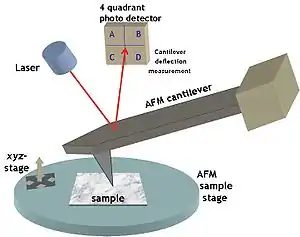
Currently, local oxidation experiments are performed with an atomic force microscope operated in contact or noncontact mode with additional circuits to apply voltage pulses between tip and sample. The local oxidation process is mediated by the formation of a water meniscus.[4]
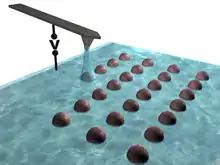
In order to perform Local Oxidation Nanolithography, the relative humidity in the AFM chamber is kept between 30% and 60%. A voltage pulse is applied between a conductive AFM tip and the sample. The applied voltage induces the formation of a water bridge between tip and sample whenever the amplitude of the voltage pulse is above a certain threshold voltage. When the liquid meniscus is created the applied voltage pulse causes an oxidation reaction by breaking the covalent bonds in the water molecules. The liquid bridge provides the oxyanions (OH−,O−) needed to form the oxide and confines the lateral extension of the region to be oxidized.
The chemical reactions that govern the Local Oxidation in a metallic substrate (M) are the following:[5]
while hydrogen gas is liberated at the AFM tip through the reduction reaction:
When the voltage pulse is off the AFM feedback forces the cantilever to recover its original oscillation amplitude withdrawing the tip from the sample and breaking the liquid meniscus. Finally the AFM continues to scan the sample thus allowing to image MOn nanostructure fabricated during the Local Oxidation process with the very same tip used for its fabrication.
The method to form liquid bridges is so precise that water meniscus diameters of 20 nm or below are easily obtained. This has led to the reproducible fabrication of sub-10 nm structures in silicon and other metallic surfaces.
Experimental setup
Local oxidation experiments can be performed with almost any kind of atomic force microscope. The key requirement is the possibility to apply voltage pulses between the tip and the sample. It is recommendable to enclose the microscope in a chamber where the atmosphere is controlled. In the simplest case, the oxidant is water vapor, which is naturally present in the air. Controlling the relative humidity generally helps to obtain more reproducible results. The size of the fabricated features depends on a number of parameters, such as the distance between the sample and the tip, the amplitude and the duration of the voltage pulse, and the relative humidity of the atmosphere.
Applications

The development of nanometer-scale lithographies is the focus of an intense research activity because progress on nanotechnology depends on the capability to fabricate, position and interconnect nanometer-scale structures.
Patterning
Local Oxidation Nanolithography allows to create a large variety of motives like dots, lines and letters with nanometer accuracy. In 2005, researchers at the Spanish National Research Council in Madrid wrote the first ten lines of Cervantes' Don Quixote on a few square micrometres of silicon.[1] This pattern versatility can be used for information storage or to design etch-resistant nanomasks in order to fabricate nanodevices as well as many other applications.
Data storage
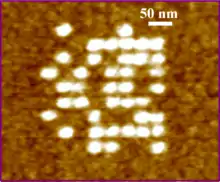
It is possible to store information using dot-like nanostructures created by the local oxidation of a surface. This storage uses the binary code considering the presence of a nanostructure as a 1 and its lack as a 0. In this way information can be stored in a small surface with a single SiO2 dot constituting a bit. In 1999 Cooper et al. demonstrated that this methods allows to obtain an information density of 1.6 Tbit/in2.[6] However, only read-only memories can be fabricated with this technique.
Molecular template growth and preferential deposition
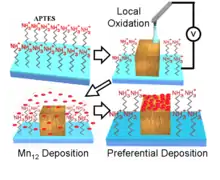
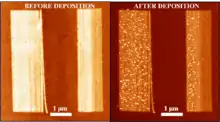
Local oxidation of silicon surfaces by noncontact atomic-force microscopy is an emerging and promising method for patterning surfaces at the nanometer scale due to its very precise control of the feature size. The features created with this technique can be used for the template growth and preferential deposition of different molecules like single molecule magnets, biomolecules and conjugated organic molecules. This method of nanopositioning is an important tool for the fabrication of new nanodevices based on the novel properties exhibited by some nanoparticles and molecules. Potential applications of single-molecule magnets (SMMs) such as Mn12 as bits for information storage or qubits for quantum computation require methods for nanoscale-controlled positioning and/or manipulation of those molecules.[7] The patterning of the Mn12 molecules on a silicon surface is achieved by first derivatizing this surface with a self-assembled monolayer of APTES, which leaves it terminated by amino groups (-NH2). Such termination electrostatically repels the Mn12 molecules. Subsequently, a pattern of silicon dioxide is defined by LON. The SMM molecules are predominantly deposited on the oxide motives because of electrostatic attraction. The electrostatic attraction between the silicon oxide fabricated by LON and the Mn12 molecules achieves the preferential deposition of this molecules with a nanoscale accuracy.
Fabrication of nanodevices
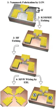
By using local oxidation nanolithography as tool for the fabrication of etch-resistant nanomasks, it is possible to fabricate nanoscale electronic devices, such as field effect transistors, single electron transistors, Josephson junctions, quantum rings or SQUIDs.[5] LON also allows to fabricate Silicon Nanowires (SiNWs) in a top-down fashion starting from silicon on insulator (SOI) wafers.[8] Local oxidation nanolithography contributes to the nanometric precision of the device fabrication. This top-down fabrication technique allows the fabrication of a large variety of SiNWs with different shapes, from angular to circular. It also allows the precise positioning of the silicon nanowires in ant desired position, making easier its integration; indeed, this technique is compatible with the standard silicon CMOS processing technology. Single crystalline silicon nanowires have already shown a great potential as ultrasensitive sensors by detecting changes in the nanowire conductivity when a specific analyte is present.[9] Local oxidation nanolithography, therefore, is a promising technique to allow the realisation of array of biosensors.
References
- Garcia, R; Martinez, RV; Martinez, J (2005). "Nano-chemistry and scanning probe nanolithographies" (PDF). Chem. Soc. Rev. 35 (1): 29–38. doi:10.1039/b501599p. PMID 16365640.
- Dagata, JA; Schneir, J; Harary, HH; Evans, CJ; Postek, MT; Bennett, J (1990). "Modification of hydrogen-passivated silicon by a scanning tunneling microscope operating in air". Appl. Phys. Lett. 56 (20): 2001. Bibcode:1990ApPhL..56.2001D. doi:10.1063/1.102999.
- Day, HC; Allee, DR (1993). "Selective area oxidation of silicon with a scanning force microscope". Appl. Phys. Lett. 62 (21): 2691. Bibcode:1993ApPhL..62.2691D. doi:10.1063/1.109259.
- Garcia, R; Calleja, M; Rohrer, H (1999). "Patterning of silicon surfaces with noncontact atomic force microscopy: Field-induced formation of nanometer-size water bridges" (PDF). J. Appl. Phys. 86 (4): 1898. Bibcode:1999JAP....86.1898G. doi:10.1063/1.370985. hdl:10261/22353.
- Tello, Marta; García, Fernando; García, Ricardo (2004). Bhushan, Bharat; Fuchs, Harald (eds.). Applied Scanning Probe Methods IV - Industrial Applications. Berlin: Springer. pp. 137–158. ISBN 3-540-26912-6.
- Cooper, EB; Manalis, SR; Fang, H; Dai, H; Matsumoto, K (1999). "Terabit-per-square-inch data storage with the atomic force microscope". Appl. Phys. Lett. 75 (22): 3566. Bibcode:1999ApPhL..75.3566C. doi:10.1063/1.125390.
- Coronado, E; Epstein, AJ (2009). "Molecular spintronics and quantum computing". J. Mater. Chem. 19 (12): 1670–1671. doi:10.1039/b901955n.
- Martinez, J; Martínez, RV; Garcia, R (2008). "Silicon Nanowire Transistors with a Channel Width of 4 nm Fabricated by Atomic Force Microscope Nanolithography". Nano Lett. 8 (11): 3636–3639. Bibcode:2008NanoL...8.3636M. doi:10.1021/nl801599k. PMID 18826289.
- Cui, Y; Wei, Q; Park, H; Lieber, CM (1999). "Nanowire Nanosensors for Highly Sensitive and Selective Detection of Biological and Chemical Species". Science. 293 (5533): 1289–92. Bibcode:2001Sci...293.1289C. doi:10.1126/science.1062711. PMID 11509722.
