Silicon carbide
Silicon carbide (SiC), also known as carborundum /kɑːrbəˈrʌndəm/, is a semiconductor containing silicon and carbon. It occurs in nature as the extremely rare mineral moissanite. Synthetic SiC powder has been mass-produced since 1893 for use as an abrasive. Grains of silicon carbide can be bonded together by sintering to form very hard ceramics that are widely used in applications requiring high endurance, such as car brakes, car clutches and ceramic plates in bulletproof vests. Electronic applications of silicon carbide such as light-emitting diodes (LEDs) and detectors in early radios were first demonstrated around 1907. SiC is used in semiconductor electronics devices that operate at high temperatures or high voltages, or both. Large single crystals of silicon carbide can be grown by the Lely method and they can be cut into gems known as synthetic moissanite.
 | |
| Names | |
|---|---|
| Preferred IUPAC name
Silicon carbide | |
| Other names
Carborundum Moissanite | |
| Identifiers | |
3D model (JSmol) |
|
| ChEBI | |
| ChemSpider | |
| ECHA InfoCard | 100.006.357 |
| EC Number |
|
| 13642 | |
| MeSH | Silicon+carbide |
PubChem CID |
|
| RTECS number |
|
| UNII | |
CompTox Dashboard (EPA) |
|
| |
| |
| Properties | |
| CSi | |
| Molar mass | 40.096 g·mol−1 |
| Appearance | Yellow to green to bluish-black, iridescent crystals[1] |
| Density | 3.16 g⋅cm−3 (hex.)[2] |
| Melting point | 2,830 °C (5,130 °F; 3,100 K)[2] (decomposes) |
| Solubility | Insoluble in water, soluble in molten alkalis and molten iron[3] |
| Electron mobility | ~900 cm2/(V⋅s) (all polytypes) |
| −12.8 × 10⁻⁶ cm3/mol[4] | |
Refractive index (nD) |
2.55 (infrared; all polytypes)[5] |
| Hazards | |
EU classification (DSD) (outdated) |
Not listed |
| NFPA 704 (fire diamond) | |
| NIOSH (US health exposure limits): | |
PEL (Permissible) |
TWA 15 mg/m3 (total) TWA 5 mg/m3 (resp)[1] |
REL (Recommended) |
TWA 10 mg/m3 (total) TWA 5 mg/m3 (resp)[1] |
IDLH (Immediate danger) |
N.D.[1] |
Except where otherwise noted, data are given for materials in their standard state (at 25 °C [77 °F], 100 kPa). | |
| Infobox references | |

History
Early experiments
Non-systematic, less-recognized and often unverified syntheses of silicon carbide include:
- César-Mansuète Despretz's passing an electric current through a carbon rod embedded in sand (1849)
- Robert Sydney Marsden's dissolution of silica in molten silver in a graphite crucible (1881)
- Paul Schuetzenberger's heating of a mixture of silicon and silica in a graphite crucible (1881)
- Albert Colson's heating of silicon under a stream of ethylene (1882).[6]
Wide-scale production

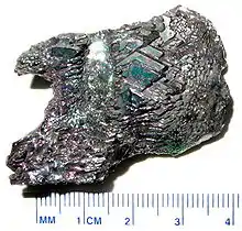
Wide-scale production is credited to Edward Goodrich Acheson in 1890.[7] Acheson was attempting to prepare artificial diamonds when he heated a mixture of clay (aluminium silicate) and powdered coke (carbon) in an iron bowl. He called the blue crystals that formed carborundum, believing it to be a new compound of carbon and aluminium, similar to corundum. In 1893, Ferdinand Henri Moissan discovered the very rare naturally occurring SiC mineral while examining rock samples found in the Canyon Diablo meteorite in Arizona. The mineral was named moissanite in his honor. Moissan also synthesized SiC by several routes, including dissolution of carbon in molten silicon, melting a mixture of calcium carbide and silica, and by reducing silica with carbon in an electric furnace.
Acheson patented the method for making silicon carbide powder on February 28, 1893.[8] Acheson also developed the electric batch furnace by which SiC is still made today and formed the Carborundum Company to manufacture bulk SiC, initially for use as an abrasive.[9] In 1900 the company settled with the Electric Smelting and Aluminum Company when a judge's decision gave "priority broadly" to its founders "for reducing ores and other substances by the incandescent method".[10] It is said that Acheson was trying to dissolve carbon in molten corundum (alumina) and discovered the presence of hard, blue-black crystals which he believed to be a compound of carbon and corundum: hence carborundum. It may be that he named the material "carborundum" by analogy to corundum, which is another very hard substance (9 on the Mohs scale).
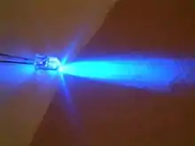
The first use of SiC was as an abrasive. This was followed by electronic applications. In the beginning of the 20th century, silicon carbide was used as a detector in the first radios.[11] In 1907 Henry Joseph Round produced the first LED by applying a voltage to a SiC crystal and observing yellow, green and orange emission at the cathode. The effect was later rediscovered by O. V. Losev in the Soviet Union in 1923.[12]
Natural occurrence
Naturally occurring moissanite is found in only minute quantities in certain types of meteorite and in corundum deposits and kimberlite. Virtually all the silicon carbide sold in the world, including moissanite jewels, is synthetic. Natural moissanite was first found in 1893 as a small component of the Canyon Diablo meteorite in Arizona by Dr. Ferdinand Henri Moissan, after whom the material was named in 1905.[13] Moissan's discovery of naturally occurring SiC was initially disputed because his sample may have been contaminated by silicon carbide saw blades that were already on the market at that time.[14]
While rare on Earth, silicon carbide is remarkably common in space. It is a common form of stardust found around carbon-rich stars, and examples of this stardust have been found in pristine condition in primitive (unaltered) meteorites. The silicon carbide found in space and in meteorites is almost exclusively the beta-polymorph. Analysis of SiC grains found in the Murchison meteorite, a carbonaceous chondrite meteorite, has revealed anomalous isotopic ratios of carbon and silicon, indicating that these grains originated outside the solar system.[15]
Production
Because natural moissanite is extremely scarce, most silicon carbide is synthetic. Silicon carbide is used as an abrasive, as well as a semiconductor and diamond simulant of gem quality. The simplest process to manufacture silicon carbide is to combine silica sand and carbon in an Acheson graphite electric resistance furnace at a high temperature, between 1,600 °C (2,910 °F) and 2,500 °C (4,530 °F). Fine SiO2 particles in plant material (e.g. rice husks) can be converted to SiC by heating in the excess carbon from the organic material.[16] The silica fume, which is a byproduct of producing silicon metal and ferrosilicon alloys, can also be converted to SiC by heating with graphite at 1,500 °C (2,730 °F).[17]
The material formed in the Acheson furnace varies in purity, according to its distance from the graphite resistor heat source. Colorless, pale yellow and green crystals have the highest purity and are found closest to the resistor. The color changes to blue and black at greater distance from the resistor, and these darker crystals are less pure. Nitrogen and aluminium are common impurities, and they affect the electrical conductivity of SiC.[18]
Pure silicon carbide can be made by the Lely process,[19] in which SiC powder is sublimed into high-temperature species of silicon, carbon, silicon dicarbide (SiC2), and disilicon carbide (Si2C) in an argon gas ambient at 2500 °C and redeposited into flake-like single crystals,[20] sized up to 2 × 2 cm, at a slightly colder substrate. This process yields high-quality single crystals, mostly of 6H-SiC phase (because of high growth temperature).
A modified Lely process involving induction heating in graphite crucibles yields even larger single crystals of 4 inches (10 cm) in diameter, having a section 81 times larger compared to the conventional Lely process.[21]
Cubic SiC is usually grown by the more expensive process of chemical vapor deposition (CVD) of silane, hydrogen and nitrogen.[18][22] Homoepitaxial and heteroepitaxial SiC layers can be grown employing both gas and liquid phase approaches.[23]
To form complex shaped SiC, preceramic polymers can be used as precursors which form the ceramic product through pyrolysis at temperatures in the range 1000–1100 °C.[24] Precursor materials to obtain silicon carbide in such a manner include polycarbosilanes, poly(methylsilyne) and polysilazanes.[25] Silicon carbide materials obtained through the pyrolysis of preceramic polymers are known as polymer derived ceramics or PDCs. Pyrolysis of preceramic polymers is most often conducted under an inert atmosphere at relatively low temperatures. Relative to the CVD process, the pyrolysis method is advantageous because the polymer can be formed into various shapes prior to thermalization into the ceramic.[26][27][28][29]
SiC can also be made into wafers by cutting a single crystal either using a diamond wire saw or by using a laser. SiC is a useful semiconductor used in power electronics.[30]
Structure and properties
 |
 |
 |
| (β)3C-SiC | 4H-SiC | (α)6H-SiC |
Silicon carbide exists in about 250 crystalline forms.[31] Through the inert atmosphere pyrolysis of preceramic polymers, silicon carbide in a glassy amorphous form is also produced.[32] The polymorphism of SiC is characterized by a large family of similar crystalline structures called polytypes. They are variations of the same chemical compound that are identical in two dimensions and differ in the third. Thus, they can be viewed as layers stacked in a certain sequence.[33]
Alpha silicon carbide (α-SiC) is the most commonly encountered polymorph, and is formed at temperatures greater than 1700 °C and has a hexagonal crystal structure (similar to Wurtzite). The beta modification (β-SiC), with a zinc blende crystal structure (similar to diamond), is formed at temperatures below 1700 °C.[34] Until recently, the beta form has had relatively few commercial uses, although there is now increasing interest in its use as a support for heterogeneous catalysts, owing to its higher surface area compared to the alpha form.
| Polytype | 3C (β) | 4H | 6H (α) |
|---|---|---|---|
| Crystal structure | Zinc blende (cubic) | Hexagonal | Hexagonal |
| Space group | T2d-F43m | C46v-P63mc | C46v-P63mc |
| Pearson symbol | cF8 | hP8 | hP12 |
| Lattice constants (Å) | 4.3596 | 3.0730; 10.053 | 3.0810; 15.12 |
| Density (g/cm3) | 3.21 | 3.21 | 3.21 |
| Bandgap (eV) | 2.36 | 3.23 | 3.05 |
| Bulk modulus (GPa) | 250 | 220 | 220 |
| Thermal conductivity (W⋅m−1⋅K−1)
@ 300 K (see [35] for temp. dependence) |
360 | 370 | 490 |
Pure SiC is colorless. The brown to black color of the industrial product results from iron impurities. The rainbow-like luster of the crystals is due to the thin-film interference of a passivation layer of silicon dioxide that forms on the surface.
The high sublimation temperature of SiC (approximately 2700 °C) makes it useful for bearings and furnace parts. Silicon carbide does not melt at any known temperature. It is also highly inert chemically. There is currently much interest in its use as a semiconductor material in electronics, where its high thermal conductivity, high electric field breakdown strength and high maximum current density make it more promising than silicon for high-powered devices.[36] SiC also has a very low coefficient of thermal expansion (4.0 × 10⁻⁶/K) and experiences no phase transitions that would cause discontinuities in thermal expansion.[18]
Electrical conductivity
Silicon carbide is a semiconductor, which can be doped n-type by nitrogen or phosphorus and p-type by beryllium, boron, aluminium, or gallium.[5] Metallic conductivity has been achieved by heavy doping with boron, aluminium or nitrogen.
Superconductivity has been detected in 3C-SiC:Al, 3C-SiC:B and 6H-SiC:B at the same temperature of 1.5 K.[34][37] A crucial difference is however observed for the magnetic field behavior between aluminium and boron doping: SiC:Al is type-II, same as Si:B. On the contrary, SiC:B is type-I. In attempt to explain this difference, it was noted that Si sites are more important than carbon sites for superconductivity in SiC. Whereas boron substitutes carbon in SiC, Al substitutes Si sites. Therefore, Al and B "see" different environments that might explain different properties of SiC:Al and SiC:B.[38]
Uses
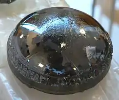
Abrasive and cutting tools
_disk.jpg.webp)
In the arts, silicon carbide is a popular abrasive in modern lapidary due to the durability and low cost of the material. In manufacturing, it is used for its hardness in abrasive machining processes such as grinding, honing, water-jet cutting and sandblasting. Particles of silicon carbide are laminated to paper to create sandpapers and the grip tape on skateboards.[39]
In 1982 an exceptionally strong composite of aluminium oxide and silicon carbide whiskers was discovered. Development of this laboratory-produced composite to a commercial product took only three years. In 1985, the first commercial cutting tools made from this alumina and silicon carbide whisker-reinforced composite were introduced into the market.[40]
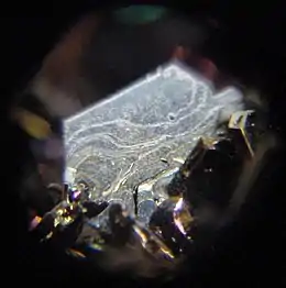
Structural material
.jpg.webp)
In the 1980s and 1990s, silicon carbide was studied in several research programs for high-temperature gas turbines in Europe, Japan and the United States. The components were intended to replace nickel superalloy turbine blades or nozzle vanes.[41] However, none of these projects resulted in a production quantity, mainly because of its low impact resistance and its low fracture toughness.[42]
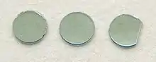
Like other hard ceramics (namely alumina and boron carbide), silicon carbide is used in composite armor (e.g. Chobham armor), and in ceramic plates in bulletproof vests. Dragon Skin, which was produced by Pinnacle Armor, used disks of silicon carbide.[43] Improved fracture toughness in SiC armor can be facilitated through the phenomenon of abnormal grain growth or AGG. The growth of abnormally long silicon carbide grains may serve to impart a toughening effect through crack-wake bridging, similar to whisker reinforcement. Similar AGG-toughening effects have been reported in Silicon nitride (Si3N4).[44]
Silicon carbide is used as a support and shelving material in high temperature kilns such as for firing ceramics, glass fusing, or glass casting. SiC kiln shelves are considerably lighter and more durable than traditional alumina shelves.[45]
In December 2015, infusion of silicon carbide nano-particles in molten magnesium was mentioned as a way to produce a new strong and plastic alloy suitable for use in aeronautics, aerospace, automobile and micro-electronics.[46]
Automobile parts
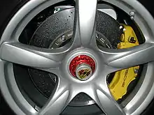
Silicon-infiltrated carbon-carbon composite is used for high performance "ceramic" brake disks, as they are able to withstand extreme temperatures. The silicon reacts with the graphite in the carbon-carbon composite to become carbon-fiber-reinforced silicon carbide (C/SiC). These brake disks are used on some road-going sports cars, supercars, as well as other performance cars including the Porsche Carrera GT, the Bugatti Veyron, the Chevrolet Corvette ZR1, the McLaren P1,[47] Bentley, Ferrari, Lamborghini and some specific high-performance Audi cars. Silicon carbide is also used in a sintered form for diesel particulate filters.[48] It's also used as an oil additive to reduce friction, emissions, and harmonics.[49][50]
Foundry crucibles
SiC is used in crucibles for holding melting metal in small and large foundry applications.[51][52]
Electric systems
The earliest electrical application of SiC was in lightning arresters in electric power systems. These devices must exhibit high resistance until the voltage across them reaches a certain threshold VT at which point their resistance must drop to a lower level and maintain this level until the applied voltage drops below VT.[53]
It was recognized early on that SiC had such a voltage-dependent resistance, and so columns of SiC pellets were connected between high-voltage power lines and the earth. When a lightning strike to the line raises the line voltage sufficiently, the SiC column will conduct, allowing strike current to pass harmlessly to the earth instead of along the power line. The SiC columns proved to conduct significantly at normal power-line operating voltages and thus had to be placed in series with a spark gap. This spark gap is ionized and rendered conductive when lightning raises the voltage of the power line conductor, thus effectively connecting the SiC column between the power conductor and the earth. Spark gaps used in lightning arresters are unreliable, either failing to strike an arc when needed or failing to turn off afterwards, in the latter case due to material failure or contamination by dust or salt. Usage of SiC columns was originally intended to eliminate the need for the spark gap in lightning arresters. Gapped SiC arresters were used for lightning-protection and sold under the GE and Westinghouse brand names, among others. The gapped SiC arrester has been largely displaced by no-gap varistors that use columns of zinc oxide pellets.[54]
Electronic circuit elements
Silicon carbide was the first commercially important semiconductor material. A crystal radio "carborundum" (synthetic silicon carbide) detector diode was patented by Henry Harrison Chase Dunwoody in 1906. It found much early use in shipboard receivers.
Power electronic devices
Silicon carbide is a semiconductor in research and early mass production providing advantages for fast, high-temperature and/or high-voltage devices. The first devices available were Schottky diodes, followed by junction-gate FETs and MOSFETs for high-power switching. Bipolar transistors and thyristors are currently developed.[36]
A major problem for SiC commercialization has been the elimination of defects: edge dislocations, screw dislocations (both hollow and closed core), triangular defects and basal plane dislocations.[55] As a result, devices made of SiC crystals initially displayed poor reverse blocking performance, though researchers have been tentatively finding solutions to improve the breakdown performance.[56] Apart from crystal quality, problems with the interface of SiC with silicon dioxide have hampered the development of SiC-based power MOSFETs and insulated-gate bipolar transistors. Although the mechanism is still unclear, nitriding has dramatically reduced the defects causing the interface problems.[57]
In 2008, the first commercial JFETs rated at 1200 V were introduced to the market,[58] followed in 2011 by the first commercial MOSFETs rated at 1200 V. JFETs are now available rated 650 V to 1700 V with resistance as low as 25 mΩ.[59] Beside SiC switches and SiC Schottky diodes (also Schottky barrier diode, SBD) in the popular TO-247 and TO-220 packages, companies started even earlier to implement the bare chips into their power electronic modules.
SiC SBD diodes found wide market spread being used in PFC circuits and IGBT power modules.[60] Conferences such as the International Conference on Integrated Power Electronics Systems (CIPS) report regularly about the technological progress of SiC power devices. Major challenges for fully unleashing the capabilities of SiC power devices are:
- Gate drive: SiC devices often require gate drive voltage levels that are different from their silicon counterparts and may be even unsymmetric, for example, +20 V and −5 V.[61]
- Packaging: SiC chips may have a higher power density than silicon power devices and are able to handle higher temperatures exceeding the silicon limit of 150 °C. New die attach technologies such as sintering are required to efficiently get the heat out of the devices and ensure a reliable interconnection.[62]
LEDs
The phenomenon of electroluminescence was discovered in 1907 using silicon carbide and the first commercial LEDs were based on SiC. Yellow LEDs made from 3C-SiC were manufactured in the Soviet Union in the 1970s[63] and blue LEDs (6H-SiC) worldwide in the 1980s.[64]
LED production soon stopped when a different material, gallium nitride, showed 10–100 times brighter emission. This difference in efficiency is due to the unfavorable indirect bandgap of SiC, whereas GaN has a direct bandgap which favors light emission. However, SiC is still one of the important LED components – it is a popular substrate for growing GaN devices, and it also serves as a heat spreader in high-power LEDs.[64]
Astronomy
The low thermal expansion coefficient, high hardness, rigidity and thermal conductivity make silicon carbide a desirable mirror material for astronomical telescopes. The growth technology (chemical vapor deposition) has been scaled up to produce disks of polycrystalline silicon carbide up to 3.5 m (11 ft) in diameter, and several telescopes like the Herschel Space Telescope are already equipped with SiC optics,[65][66] as well the Gaia space observatory spacecraft subsystems are mounted on a rigid silicon carbide frame, which provides a stable structure that will not expand or contract due to heat.
Thin filament pyrometry
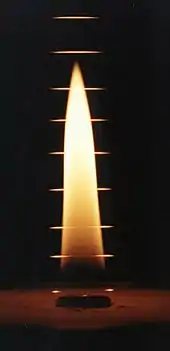
Silicon carbide fibers are used to measure gas temperatures in an optical technique called thin filament pyrometry. It involves the placement of a thin filament in a hot gas stream. Radiative emissions from the filament can be correlated with filament temperature. Filaments are SiC fibers with a diameter of 15 micrometers, about one fifth that of a human hair. Because the fibers are so thin, they do little to disturb the flame and their temperature remains close to that of the local gas. Temperatures of about 800–2500 K can be measured.[67][68]
Heating elements
References to silicon carbide heating elements exist from the early 20th century when they were produced by Acheson's Carborundum Co. in the U.S. and EKL in Berlin. Silicon carbide offered increased operating temperatures compared with metallic heaters. Silicon carbide elements are used today in the melting of glass and non-ferrous metal, heat treatment of metals, float glass production, production of ceramics and electronics components, igniters in pilot lights for gas heaters, etc.[69]
Nuclear fuel particles and cladding
Silicon carbide is an important material in TRISO-coated fuel particles, the type of nuclear fuel found in high temperature gas cooled reactors such as the Pebble Bed Reactor. A layer of silicon carbide gives coated fuel particles structural support and is the main diffusion barrier to the release of fission products.[70]
Silicon carbide composite material has been investigated for use as a replacement for Zircaloy cladding in light water reactors. One of the reasons for this investigation is that, Zircaloy experiences hydrogen embrittlement as a consequence of the corrosion reaction with water. This produces a reduction in fracture toughness with increasing volumetric fraction of radial hydrides. This phenomenon increases drastically with increasing temperature to the detriment of the material.[71] Silicon carbide cladding does not experience this same mechanical degradation, but instead retains strength properties with increasing temperature. The composite consists of SiC fibers wrapped around a SiC inner layer and surrounded by an SiC outer layer.[72] Problems have been reported with the ability to join the pieces of the SiC composite.[73]
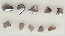
Jewelry
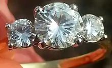
As a gemstone used in jewelry, silicon carbide is called "synthetic moissanite" or just "moissanite" after the mineral name. Moissanite is similar to diamond in several important respects: it is transparent and hard (9–9.5 on the Mohs scale, compared to 10 for diamond), with a refractive index between 2.65 and 2.69 (compared to 2.42 for diamond). Moissanite is somewhat harder than common cubic zirconia. Unlike diamond, moissanite can be strongly birefringent. For this reason, moissanite jewels are cut along the optic axis of the crystal to minimize birefringent effects. It is lighter (density 3.21 g/cm3 vs. 3.53 g/cm3), and much more resistant to heat than diamond. This results in a stone of higher luster, sharper facets, and good resilience. Loose moissanite stones may be placed directly into wax ring moulds for lost-wax casting, as can diamond,[74] as moissanite remains undamaged by temperatures up to 1,800 °C (3,270 °F). Moissanite has become popular as a diamond substitute, and may be misidentified as diamond, since its thermal conductivity is closer to diamond than any other substitute. Many thermal diamond-testing devices cannot distinguish moissanite from diamond, but the gem is distinct in its birefringence and a very slight green or yellow fluorescence under ultraviolet light. Some moissanite stones also have curved, string-like inclusions, which diamonds never have.[75]
Steel production
Silicon carbide, dissolved in a basic oxygen furnace used for making steel, acts as a fuel. The additional energy liberated allows the furnace to process more scrap with the same charge of hot metal. It can also be used to raise tap temperatures and adjust the carbon and silicon content. Silicon carbide is cheaper than a combination of ferrosilicon and carbon, produces cleaner steel and lower emissions due to low levels of trace elements, has a low gas content, and does not lower the temperature of steel.[76]
Catalyst support
The natural resistance to oxidation exhibited by silicon carbide, as well as the discovery of new ways to synthesize the cubic β-SiC form, with its larger surface area, has led to significant interest in its use as a heterogeneous catalyst support. This form has already been employed as a catalyst support for the oxidation of hydrocarbons, such as n-butane, to maleic anhydride.[77][78]
Carborundum printmaking
Silicon carbide is used in carborundum printmaking – a collagraph printmaking technique. Carborundum grit is applied in a paste to the surface of an aluminium plate. When the paste is dry, ink is applied and trapped in its granular surface, then wiped from the bare areas of the plate. The ink plate is then printed onto paper in a rolling-bed press used for intaglio printmaking. The result is a print of painted marks embossed into the paper.
Carborundum grit is also used in stone Lithography. Its uniform particle size allows it to be used to "Grain" a stone which removes the previous image. In a similar process to sanding, coarser grit Carborundum is applied to the stone and worked with a Levigator, then gradually finer and finer grit is applied until the stone is clean. This creates a grease sensitive surface.[79]
Graphene production
Silicon carbide can be used in the production of graphene because of its chemical properties that promote the epitaxial production of graphene on the surface of SiC nanostructures.
When it comes to its production, silicon is used primarily as a substrate to grow the graphene. But there are actually several methods that can be used to grow the graphene on the silicon carbide. The confinement controlled sublimation (CCS) growth method consists of a SiC chip that is heated under vacuum with graphite. Then the vacuum is released very gradually to control the growth of graphene. This method yields the highest quality graphene layers. But other methods have been reported to yield the same product as well.
Another way of growing graphene would be thermally decomposing SiC at a high temperature within a vacuum.[80] But this method turns out to yield graphene layers that contain smaller grains within the layers.[81] So there have been efforts to improve the quality and yield of graphene. One such method is to perform ex situ graphitization of silicon terminated SiC in an atmosphere consisting of argon. This method has proved to yield layers of graphene with larger domain sizes than the layer that would be attainable via other methods. This new method can be very viable to make higher quality graphene for a multitude of technological applications.
When it comes to understanding how or when to use these methods of graphene production, most of them mainly produce or grow this graphene on the SiC within a growth enabling environment. It is utilized most often at rather higher temperatures (such as 1300˚C) because of SiC thermal properties.[82] However, there have been certain procedures that have been performed and studied that could potentially yield methods that use lower temperatures to help manufacture graphene. More specifically this different approach to graphene growth has been observed to produce graphene within a temperature environment of around 750˚C. This method entails the combination of certain methods like chemical vapor deposition (CVD) and surface segregation. And when it comes to the substrate, the procedure would consist of coating a SiC substrate with thin films of a transition metal. And after the rapid heat treating of this substance, the carbon atoms would then become more abundant at the surface interface of the transition metal film which would then yield graphene. And this process was found to yield graphene layers that were more continuous throughout the substrate surface.[83]
Quantum physics
Silicon carbide can host point defects in the crystal lattice which are known as color centers. These defects can produce single photons on demand and thus serve as a platform for single-photon source. Such a device is a fundamental resource for many emerging applications of quantum information science. If one pumps a color center via an external optical source or electrical current, the color center will be brought to the excited state and then relax with the emission of one photon.[84][85]
One well known point defect in silicon carbide is the divacancy which has a similar electronic structure as the nitrogen-vacancy center in diamond. In 4H-SiC, the divacancy has four different configurations which correspond to four zero-phonon lines (ZPL). These ZPL values are written using the notation VSi-VC and the unit eV: hh(1.095), kk(1.096), kh(1.119), and hk(1.150).[86]
Fishing rod guides
Silicon carbide is used in the manufacturing of fishing guides because of its durability and wear resistance.[87] Silicon Carbide rings are fit into a guide frame, typically made from stainless steel or titanium which keep the line from touching the rod blank. The rings provide a low friction surface which improves casting distance while providing adequate hardness that prevents abrasion from braided fishing line.[88]
References
- NIOSH Pocket Guide to Chemical Hazards. "#0555". National Institute for Occupational Safety and Health (NIOSH).
- Haynes, William M., ed. (2011). CRC Handbook of Chemistry and Physics (92nd ed.). Boca Raton, FL: CRC Press. p. 4.88. ISBN 1439855110.
- Pubchem. "Silicon carbide". pubchem.ncbi.nlm.nih.gov. Retrieved 2018-11-27.
- Haynes, William M., ed. (2011). CRC Handbook of Chemistry and Physics (92nd ed.). Boca Raton, FL: CRC Press. p. 4.135. ISBN 1439855110.
- "Properties of Silicon Carbide (SiC)". Ioffe Institute. Retrieved 2009-06-06.
- Weimer, A. W. (1997). Carbide, nitride, and boride materials synthesis and processing. Springer. p. 115. ISBN 978-0-412-54060-8.
- Encyclopædia Britannica, eb.com
- Acheson, G. (1893) U.S. Patent 492,767 "Production of artificial crystalline carbonaceous material"
- "The Manufacture of Carborundum- a New Industry". Scientific American. April 7, 1894. Archived from the original on January 23, 2009. Retrieved 2009-06-06.
- Mabery, Charles F. (1900). "Notes, On Carborundum". Journal of the American Chemical Society. XXII (Part II): 706–707. doi:10.1021/ja02048a014. Retrieved 2007-10-28.
- Dunwoody, Henry H.C. (1906) U.S. Patent 837,616 Wireless telegraph system (silicon carbide detector)
- Hart, Jeffrey A.; Stefanie Ann Lenway; Thomas Murtha. "A History of Electroluminescent Displays".
- Moissan, Henri (1904). "Nouvelles recherches sur la météorité de Cañon Diablo". Comptes rendus. 139: 773–86.
- Di Pierro S.; Gnos E.; Grobety B.H.; Armbruster T.; Bernasconi S.M. & Ulmer P. (2003). "Rock-forming moissanite (natural α-silicon carbide)". American Mineralogist. 88 (11–12): 1817–21. Bibcode:2003AmMin..88.1817D. doi:10.2138/am-2003-11-1223. S2CID 128600868.
- Kelly, Jim. "The Astrophysical Nature of Silicon Carbide". University College London. Archived from the original on May 4, 2017. Retrieved 2009-06-06.
- Vlasov, A.S.; et al. (1991). "Obtaining silicon carbide from rice husks". Refractories and Industrial Ceramics. 32 (9–10): 521–523. doi:10.1007/bf01287542. S2CID 135784055.
- Zhong, Y.; Shaw, Leon L.; Manjarres, Misael & Zawrah, Mahmoud F. (2010). "Synthesis of Silicon Carbide Nanopowder Using Silica Fume". Journal of the American Ceramic Society. 93 (10): 3159–3167. doi:10.1111/j.1551-2916.2010.03867.x.
- Harris, Gary Lynn (1995). Properties of silicon carbide. IET. p. 19; 170–180. ISBN 978-0-85296-870-3.
- Lely, Jan Anthony (1955). "Darstellung von Einkristallen von Silicium Carbid und Beherrschung von Art und Menge der eingebauten Verunreinigungen". Berichte der Deutschen Keramischen Gesellschaft. 32: 229–236.
- Lely SiC Wafers. Nitride-crystals.com. Retrieved on 2013-05-04.
- Ohtani, N.; et al. (2001). Nippon Steel Technical Report no. 84 : Large high-quality silicon carbide substrates (PDF). Archived from the original (PDF) on 2010-12-17.
- Byrappa, K.; Ohachi, T. (2003). Crystal growth technology. Springer. pp. 180–200. ISBN 978-3-540-00367-0.
- Bakin, Andrey S. (2006). "SiC Homoepitaxy and Heteroepitaxy". In M. Shur; S. Rumyantsev; M. Levinshtein (eds.). SiC materials and devices. 1. World Scientific. pp. 43–76. ISBN 978-981-256-835-9.
- AM of Ceramics from Preceramic Polymers Published in Additive Manufacturing 2019, vol. 27 pp 80-90
- Europe Makes Ceramics Preceramics
- Park, Yoon-Soo (1998). SiC materials and devices. Academic Press. pp. 20–60. ISBN 978-0-12-752160-2.
- Pitcher, M. W.; Joray, S. J.; Bianconi, P. A. (2004). "Smooth Continuous Films of Stoichiometric Silicon Carbide from Poly(methylsilyne)". Advanced Materials. 16 (8): 706–709. doi:10.1002/adma.200306467.
- Bunsell, A. R.; Piant, A. (2006). "A review of the development of three generations of small diameter silicon carbide fibres". Journal of Materials Science. 41 (3): 823–839. Bibcode:2006JMatS..41..823B. doi:10.1007/s10853-006-6566-z. S2CID 135586321.
- Laine, Richard M.; Babonneau, Florence (1993). "Preceramic polymer routes to silicon carbide". Chemistry of Materials. 5 (3): 260–279. doi:10.1021/cm00027a007.
- https://www.disco.co.jp/kabra/index_eg.html
- Cheung, Rebecca (2006). Silicon carbide microelectromechanical systems for harsh environments. Imperial College Press. p. 3. ISBN 978-1-86094-624-0.
- Additive Manufacturing of Ceramics from Preceramic Polymers Published in Additive Manufacturing 2019, vol. 27 pp 80-90
- Morkoç, H.; Strite, S.; Gao, G. B.; Lin, M. E.; Sverdlov, B.; Burns, M. (1994). "Large-band-gap SiC, III-V nitride, and II-VI ZnSe-based semiconductor device technologies". Journal of Applied Physics. 76 (3): 1363. Bibcode:1994JAP....76.1363M. doi:10.1063/1.358463.
- Muranaka, T.; Kikuchi, Yoshitake; Yoshizawa, Taku; Shirakawa, Naoki; Akimitsu, Jun (2008). "Superconductivity in carrier-doped silicon carbide". Sci. Technol. Adv. Mater. 9 (4): 044204. Bibcode:2008STAdM...9d4204M. doi:10.1088/1468-6996/9/4/044204. PMC 5099635. PMID 27878021.
- Silicon Carbide. Thermal properties. Ioffe Institute Semiconductors Database.
- Bhatnagar, M.; Baliga, B.J. (March 1993). "Comparison of 6H-SiC, 3C-SiC, and Si for power devices". IEEE Transactions on Electron Devices. 40 (3): 645–655. Bibcode:1993ITED...40..645B. doi:10.1109/16.199372.
- Kriener, M.; Muranaka, Takahiro; Kato, Junya; Ren, Zhi-An; Akimitsu, Jun; Maeno, Yoshiteru (2008). "Superconductivity in heavily boron-doped silicon carbide". Sci. Technol. Adv. Mater. 9 (4): 044205. arXiv:0810.0056. Bibcode:2008STAdM...9d4205K. doi:10.1088/1468-6996/9/4/044205. PMC 5099636. PMID 27878022.
- Yanase, Y. & Yorozu, N. (2008). "Superconductivity in compensated and uncompensated semiconductors". Sci. Technol. Adv. Mater. 9 (4): 044201. Bibcode:2008STAdM...9d4201Y. doi:10.1088/1468-6996/9/4/044201. PMC 5099632. PMID 27878018.
- Fuster, Marco A. (1997) "Skateboard grip tape", U.S. Patent 5,622,759
- Bansal, Narottam P. (2005). Handbook of ceramic composites. Springer. p. 312. ISBN 978-1-4020-8133-0.
- "Production of Silicon Carbide". siliconcarbide.net.
- "Ceramics for turbine engines". unipass.com. Archived from the original on 2009-04-06. Retrieved 2009-06-06.
- "Dragon Skin – Most Protective Body Armor – Lightweight". Future Firepower. Archived from the original on 2012-02-17. Retrieved 2009-06-06.
- Abnormal Grain Growth in Journal of Crystal Growth 2012, Volume 359, Pages 83-91
- "Silicon Carbide". Ceramic Arts Daily.
- UCLA researchers create exceptionally strong and lightweight new metal
- "Top 10 Fast Cars". topmost10.com. Archived from the original on 2009-03-26. Retrieved 2009-06-06.
- O'Sullivan, D.; Pomeroy, M.J.; Hampshire, S.; Murtagh, M.J. (2004). "Degradation resistance of silicon carbide diesel particulate filters to diesel fuel ash deposits". MRS Proceedings. 19 (10): 2913–2921. Bibcode:2004JMatR..19.2913O. doi:10.1557/JMR.2004.0373.
- "SiC Lubrication". Cerma.
- Studt, P. (1987). "Influence of lubricating oil additives on friction of ceramics under conditions of boundary lubrication". Wear. 115 (1–2): 185–191. doi:10.1016/0043-1648(87)90208-0.
- Friedrichs, Peter; Kimoto, Tsunenobu; Ley, Lothar; Pensl, Gerhard (2011). Silicon Carbide: Volume 1: Growth, Defects, and Novel Applications. John Wiley & Sons. pp. 49–. ISBN 978-3-527-62906-0.
- Brown, John (1999). Foseco Non-Ferrous Foundryman's Handbook. Butterworth-Heinemann. pp. 52–. ISBN 978-0-08-053187-8.
- Whitaker, Jerry C. (2005). The electronics handbook. CRC Press. p. 1108. ISBN 978-0-8493-1889-4.
- Bayliss, Colin R. (1999). Transmission and distribution electrical engineering. Newnes. p. 250. ISBN 978-0-7506-4059-6.
- Chen, H.; Raghothamachar, Balaji; Vetter, William; Dudley, Michael; Wang, Y.; Skromme, B.J. (2006). "Effects of defect types on the performance of devices fabricated on a 4H-SiC homoepitaxial layer". Mater. Res. Soc. Symp. Proc. 911: 169. doi:10.1557/PROC-0911-B12-03.
- Madar, Roland (26 August 2004). "Materials science: Silicon carbide in contention". Nature. 430 (7003): 974–975. Bibcode:2004Natur.430..974M. doi:10.1038/430974a. PMID 15329702. S2CID 4328365.
- Chen, Z.; Ahyi, A.C.; Zhu, X.; Li, M.; Isaacs-Smith, T.; Williams, J.R.; Feldman, L.C. (2010). "MOS Characteristics of C-Face 4H-SiC". J. Of Elec. Mat. 39 (5): 526–529. Bibcode:2010JEMat..39..526C. doi:10.1007/s11664-010-1096-5. S2CID 95074081.
- "At 1200 V and 45 milliohms, SemiSouth introduces the industry's lowest resistance SiC power transistor for efficient power management". Reuters (Press release). 5 May 2011. Archived from the original on 15 March 2016.
- "SiC JFETs Archives". United Silicon Carbide Inc. Retrieved 2021-01-11.
- "Cree launches industry's first commercial silicon carbide power MOSFET; destined to replace silicon devices in high-voltage (≥ 1200 V) power electronics" (Press release). Cree. 17 January 2011.
- Meißer, Michael (2013). Resonant Behaviour of Pulse Generators for the Efficient Drive of Optical Radiation Sources Based on Dielectric Barrier Discharges. KIT Scientific Publishing. p. 94. ISBN 978-3-7315-0083-4.
- Horio, Masafumi; Iizuka, Yuji; Ikeda, Yoshinari (2012). "Packaging Technologies for SiC Power Modules" (PDF). Fuji Electric Review. 58 (2): 75–78.
- Klipstein, Don. "Yellow SiC LED". Retrieved 6 June 2009.
- Stringfellow, Gerald B. (1997). High brightness light emitting diodes. Academic Press. pp. 48, 57, 425. ISBN 978-0-12-752156-5.
- "The largest telescope mirror ever put into space". European Space Agency. Retrieved 2009-06-06.
- Petrovsky, Gury T.; Tolstoy, Michael N.; Lubarsky, Sergey V.; Khimitch, Yuri P.; Robb, Paul N.; Tolstoy; Lubarsky; Khimitch; Robb (1994). Stepp, Larry M. (ed.). "2.7-meter-diameter silicon carbide primary mirror for the SOFIA telescope". Proc. SPIE. Advanced Technology Optical Telescopes V. 2199: 263. Bibcode:1994SPIE.2199..263P. doi:10.1117/12.176195. S2CID 120854083.CS1 maint: multiple names: authors list (link)
- "Thin-Filament Pyrometry Developed for Measuring Temperatures in Flames". NASA. Archived from the original on 2012-03-15. Retrieved 2009-06-06.CS1 maint: bot: original URL status unknown (link)
- Maun, Jignesh D.; Sunderland, P. B.; Urban, D. L. (2007). "Thin-filament pyrometry with a digital still camera" (PDF). Applied Optics. 46 (4): 483–8. Bibcode:2007ApOpt..46..483M. doi:10.1364/AO.46.000483. hdl:1903/3602. PMID 17230239.
- Deshmukh, Yeshvant V. (2005). Industrial heating: principles, techniques, materials, applications, and design. CRC Press. pp. 383–393. ISBN 978-0-8493-3405-4.
- López-Honorato, E.; Tan, J.; Meadows, P. J.; Marsh, G.; Xiao, P. (2009). "TRISO coated fuel particles with enhanced SiC properties". Journal of Nuclear Materials. 392 (2): 219–224. Bibcode:2009JNuM..392..219L. doi:10.1016/j.jnucmat.2009.03.013.
- Bertolino, Meyer, G. (2002). "Degradation of the mechanical properties of Zircaloy-4 due to hydrogen embrittlement". Journal of Alloys and Compounds. 330–332: 408–413. doi:10.1016/S0925-8388(01)01576-6.
- Carpenter, David; Ahn, K.; Kao, S.P.; Hejzlar, Pavel; Kazimi, Mujid S. "Assessment of Silicon Carbide Cladding for High Performance Light Water Reactors". Nuclear Fuel Cycle Program, Volume MIT-NFC-TR-098 (2007). Archived from the original on 2012-04-25. Retrieved 2011-10-13.
- Ames, Nate (June 17, 2010). "SiC Fuel Cladding". Nuclear Fabrication Consortium, nuclearfabrication.org. Archived from the original on April 25, 2012. Retrieved 2011-10-13.
- Teague, Tyler. Casting Metal Directly onto Stones, Jett Industries
- O'Donoghue, M. (2006). Gems. Elsevier. p. 89. ISBN 978-0-7506-5856-0.
- "Silicon carbide (steel industry)". Archived from the original on 2012-02-04. Retrieved 2009-06-06.
- Rase, Howard F. (2000). Handbook of commercial catalysts: heterogeneous catalysts. CRC Press. p. 258. ISBN 978-0-8493-9417-1.
- Singh, S. K.; Parida, K. M.; Mohanty, B. C.; Rao, S. B. (1995). "High surface area silicon carbide from rice husk: A support material for catalysts". Reaction Kinetics and Catalysis Letters. 54 (1): 29–34. doi:10.1007/BF02071177. S2CID 95550450.
- "Printmaking". Bircham Gallery, birchamgallery.co.uk. Retrieved 2009-07-31.
- Ruan, Ming; Hu, Yike; Guo, Zelei; Dong, Rui; Palmer, James; Hankinson, John; Berger, Claire; Heer, Walt A. de (December 2012). "Epitaxial graphene on silicon carbide: Introduction to structured graphene" (PDF). MRS Bulletin. 37 (12): 1138–1147. doi:10.1557/mrs.2012.231. ISSN 0883-7694.
- Emtsev, Konstantin V.; Bostwick, Aaron; Horn, Karsten; Jobst, Johannes; Kellogg, Gary L.; Ley, Lothar; McChesney, Jessica L.; Ohta, Taisuke; Reshanov, Sergey A. (2009-02-08). "Towards wafer-size graphene layers by atmospheric pressure graphitization of silicon carbide". Nature Materials. 8 (3): 203–207. Bibcode:2009NatMa...8..203E. doi:10.1038/nmat2382. hdl:11858/00-001M-0000-0010-FA05-E. ISSN 1476-1122. PMID 19202545.
- de Heer, Walt A.; Berger, Claire; Wu, Xiaosong; First, Phillip N.; Conrad, Edward H.; Li, Xuebin; Li, Tianbo; Sprinkle, Michael; Hass, Joanna (July 2007). "Epitaxial graphene". Solid State Communications. 143 (1–2): 92–100. arXiv:0704.0285. Bibcode:2007SSCom.143...92D. doi:10.1016/j.ssc.2007.04.023. ISSN 0038-1098. S2CID 44542277.
- Juang, Zhen-Yu; Wu, Chih-Yu; Lo, Chien-Wei; Chen, Wei-Yu; Huang, Chih-Fang; Hwang, Jenn-Chang; Chen, Fu-Rong; Leou, Keh-Chyang; Tsai, Chuen-Horng (2009-07-01). "Synthesis of graphene on silicon carbide substrates at low temperature". Carbon. 47 (8): 2026–2031. doi:10.1016/j.carbon.2009.03.051. ISSN 0008-6223.
- Lohrmann, A.; Iwamoto, N.; Bodrog, Z.; Castalletto, S.; Ohshima, T.; Karle, T.J.; Gali, A.; Prawer, S.; McCallum, J.C.; Johnson, B.C. (2015). "Single-photon emitting diode in silicon carbide". Nature Communications. 6: 7783. arXiv:1503.07566. Bibcode:2015NatCo...6.7783L. doi:10.1038/ncomms8783. PMID 26205309. S2CID 205338373.
- Khramtsov, I.A.; Vyshnevyy, A.A.; Fedyanin, D. Yu. (2018). "Enhancing the brightness of electrically driven single-photon sources using color centers in silicon carbide". NPJ Quantum Information. 4: 15. Bibcode:2018npjQI...4...15K. doi:10.1038/s41534-018-0066-2.
- Davidsson, J.; Ivády, V.; Armiento, R.; Son, N.T.; Gali, A.; Abrikosov, I. A. (2018). "First principles predictions of magneto-optical data for semiconductor point defect identification: the case of divacancy defects in 4H–SiC". New Journal of Physics. 20 (2): 023035. arXiv:1708.04508. Bibcode:2018NJPh...20b3035D. doi:10.1088/1367-2630/aaa752. S2CID 4867492.
- "The best spinning rod". Retrieved 2020-06-27.
- C. Boyd Pfeiffer (15 January 2013). Complete Book of Rod Building and Tackle Making. Rowman & Littlefield. ISBN 978-0-7627-9502-4.
External links
| Wikimedia Commons has media related to Silicon carbide. |
| Wikisource has the text of the 1911 Encyclopædia Britannica article Carborundum. |
- A Brief History of Silicon Carbide Dr J F Kelly, University of London
- Material Safety Data Sheet for Silicon Carbide
- Moissanite on Mindat.org
- CDC – NIOSH Pocket Guide to Chemical Hazards
| Authority control |
|---|