Q-Bus
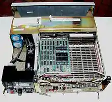
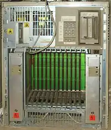
The Q-bus,[1] also known as the LSI-11 Bus, is one of several bus technologies used with PDP and MicroVAX computer systems previously manufactured by the Digital Equipment Corporation of Maynard, Massachusetts.
| Q-Bus | |
| Created by | Digital Equipment Corporation |
|---|---|
| Width in bits | 8 or 16-bit data, 16-bit address extended to 22-bit |
| No. of devices | 127 in theory, ~20 in practice |
| Style | Parallel |
The Q-bus is a less expensive version of Unibus using multiplexing so that address and data signals share the same wires. This allows both a physically smaller and less-expensive implementation of essentially the same functionality.
Over time, the physical address range of the Q-bus was expanded from 16 to 18 and then 22 bits. Block transfer modes were also added to the Q-bus.
Main features of the Q-bus


Like the Unibus before it, the Q-bus uses:
- Memory-mapped I/O
- Byte addressing
- A strict master-slave relationship between devices on the bus
- Asynchronous signaling
Memory-mapped I/O means that data cycles between any two devices, whether CPU, memory, or I/O devices, use the same protocols. On the Unibus, a range of physical addresses are dedicated for I/O devices. The Q-bus simplifies this design by providing a specific signal (originally called BBS7, Bus Bank Select 7 but later generalized to be called BBSIO, Bus Bank Select I/O) that selects the range of addresses used by the I/O devices.
Byte addressing means that the physical address passed on the Unibus is interpreted as the address of a byte-sized quantity of data. Because the bus actually contains a data path that is two bytes wide, address bit [0] is subject to special interpretation and data on the bus has to travel in the correct byte lanes.
A strict Master-Slave relationship means that at any point in time, only one device can be the Master of the Q-bus. This master device can initiate data transactions which can then be responded to by a maximum of one selected slave device. (This had no effect on whether a given bus cycle is reading or writing data; the bus master can command either type of transaction.) At the end of the bus cycle, a bus arbitration protocol then selects the next device to be given mastery of the bus.
Asynchronous signaling means that the bus has no fixed cycle time; the duration of any particular data transfer cycle on the bus is determined solely by the master and slave devices participating in the current data cycle. These devices use handshake signals to control the timing of the data cycle. Timeout logic within the master device limits the maximum allowed length of any given bus cycle.
Depending on its generation, the Q-bus contains 16, 18, or 22 BDAL (Bus Data/Address Line) lines. 16, 18, or 22 BDAL lines are used for the physical address portion of each bus cycle. Eight or 16 DBAL lines are then re-used for the data portion(s) of each bus cycle. Newer generations of the bus allow block mode transfer where a single bus address can be followed by more than one data cycle (with the transfers taking place at consecutive bus addresses). Because the address portion of each bus cycle can not transfer data, the use of block mode means fewer address cycles and more time for data cycles, allowing increased bus data transfer bandwidth.
Bus mastery is awarded based on an I/O card's topological proximity to the bus arbitrator (at the logical front of the bus); closer cards are granted priority over further cards.
Interrupts can be delivered to the Interrupt Fielding Processor at any of four interrupt priority levels. Within a given level, the cards closer to the IFP (at the front of the bus) take priority over cards further back on the bus. Interrupts are vectored: a card requesting an interrupt has its interrupt vector read by the IFP. In this way, the interrupts from all I/O cards in the system can be distinguished with no ambiguity.
Logic minimization
As with the Unibus, the signaling was carefully optimized so that the minimum amount of logic is required across the entire bus system. Asynchronous signaling is used but de-skewing of addresses and data is the responsibility of the current bus master, minimizing the complexity of the bus slave devices. The responsibility for timing-out failed bus cycles also is placed in the master devices. Similarly, the complexities of handling interrupt transactions are concentrated into the single Interrupt-Fielding Processor (the PDP-11 or VAX-11 computer) in the system.
Compatibility
The design of the Q-bus was very closely related to the design of the Unibus both in spirit and in detailed implementation. Adapters were available from Digital and from third parties that allow Q-bus devices to be connected to Unibus-based computers and vice versa. A number of I/O devices were available in either Unibus or Q-bus flavors; some of these devices have minor differences while many others were essentially identical.
Soviet clones
In Soviet systems (see 1801 series CPU), the Q-Bus architecture is called МПИ (Магистральный Параллельный Интерфейс, or parallel bus interface). Its main difference is that it supports up to four processors on the same bus. Otherwise it is completely binary and electrically compatible with the standard Q-Bus, except for the physical layout of connectors.
Cycle Types
The Q-Bus supports 6 basic transaction types
DATI Data in - master read - note no DATIB (not required)
DATO Data out - master write
DATOB Data out (byte)
DATIO Data in/out
DATIOB Data in/out (byte)
IAK Interrupt Acknowledge
Interfaces
A wide range of interface cards are available for the Q-Bus.
External links
- HP OpenVMS :: Q-Bus Hardware, HoffmanLabs
- DIY, The Lab - Q-Bus Beispielplatine, Selbstgebaute Q-BUS Platinen
- DEC STD 160: LSI-11 Bus Specification
- PDP-11 Bus Handbook UNIBUS and LSI-11 Bus
References
- Schmidt, Atlant G.,Unibus,Q-Bus and VAXBI Bus, in Digital bus handbook, Di Giacomo Joseph Ed., McGraw Hill, 1990 ISBN 0070169233