Magnetic-core memory
Magnetic-core memory was the predominant form of random-access computer memory for 20 years between about 1955 and 1975. Such memory is often just called core memory, or, informally, core.
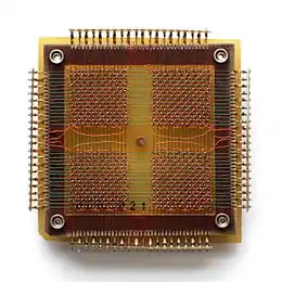
Core memory uses toroids (rings) of a hard magnetic material (usually a semi-hard ferrite) as transformer cores, where each wire threaded through the core serves as a transformer winding. Three or four wires pass through each core. Magnetic hysteresis allows each of the cores to "remember", or store a state.
Each core stores one bit of information. A core can be magnetized in either the clockwise or counter-clockwise direction. The value of the bit stored in a core is zero or one according to the direction of that core's magnetization. Electric current pulses in some of the wires through a core allow the direction of the magnetization in that core to be set in either direction, thus storing a one or a zero. Another wire through each core, the sense wire, is used to detect whether the core changed state.
The process of reading the core causes the core to be reset to a zero, thus erasing it. This is called destructive readout. When not being read or written, the cores maintain the last value they had, even if the power is turned off. Therefore they are a type of non-volatile memory.
Using smaller cores and wires, the memory density of core slowly increased, and by the late 1960s a density of about 32 kilobits per cubic foot (about 0.9 kilobits per litre) was typical. However, reaching this density required extremely careful manufacture, almost always carried out by hand in spite of repeated major efforts to automate the process. The cost declined over this period from about $1 per bit to about 1 cent per bit. The introduction of the first semiconductor memory chips in the late 1960s, which initially created static random-access memory (SRAM), began to erode the market for core memory. The first successful dynamic random-access memory (DRAM), the Intel 1103, followed in 1970. Its availability in quantity at 1 cent per bit marked the beginning of the end for core memory.[1]
Improvements in semiconductor manufacturing led to rapid increases in storage capacity and decreases in price per kilobyte, while the costs and specs of core memory changed little. Core memory was driven from the market gradually between 1973 and 1978.
Depending on how it was wired, core memory could be exceptionally reliable. Read-only core rope memory, for example, was used on the mission-critical Apollo Guidance Computer essential to NASA's successful Moon landings.
Although core memory is obsolete, computer memory is still sometimes called "core" even though it is made of semiconductors, particularly by people who had worked with machines having actual core memory. The files that result from saving the entire contents of memory to disk for inspection, which is nowadays commonly performed automatically when a major error occurs in a computer program, are still called "core dumps".
History
Developers
The basic concept of using the square hysteresis loop of certain magnetic materials as a storage or switching device was known from the earliest days of computer development. Much of this knowledge had developed due to an understanding of transformers, which allowed amplification and switch-like performance when built using certain materials. The stable switching behavior was well known in the electrical engineering field, and its application in computer systems was immediate. For example, J. Presper Eckert and Jeffrey Chuan Chu had done some development work on the concept in 1945 at the Moore School during the ENIAC efforts.[2]
Frederick Viehe applied for various patents on the use of transformers for building digital logic circuits in place of relay logic beginning in 1947. A fully developed core system was patented in 1947, and later purchased by IBM in 1956.[3] This development was little-known, however, and the mainstream development of core is normally associated with three independent teams.
Substantial work in the field was carried out by the Shanghai-born American physicists An Wang and Way-Dong Woo, who created the pulse transfer controlling device in 1949.[4][5] The name referred to the way that the magnetic field of the cores could be used to control the switching of current; his patent focused on using cores to create delay-line or shift-register memory systems. Wang and Woo were working at Harvard University's Computation Laboratory at the time, and the university was not interested in promoting inventions created in their labs. Wang was able to patent the system on his own.

The MIT Project Whirlwind computer required a fast memory system for real-time aircraft tracking. At first, an array of Williams tubes—a storage system based on cathode ray tubes—was used, but proved temperamental and unreliable. Several researchers in the late 1940s conceived the idea of using magnetic cores for computer memory, but MIT computer engineer Jay Forrester received the principal patent for his invention of the coincident-core memory that enabled the 3D storage of information.[6][7] William Papian of Project Whirlwind cited one of these efforts, Harvard's "Static Magnetic Delay Line", in an internal memo. The first core memory of 32 x 32 x 16 bits was installed on Whirlwind in the summer of 1953. Papian stated: "Magnetic-Core Storage has two big advantages: (1) greater reliability with a consequent reduction in maintenance time devoted to storage; (2) shorter access time (core access time is 9 microseconds: tube access time is approximately 25 microseconds) thus increasing the speed of computer operation."[8]
In April 2011, Forrester recalled, "the Wang use of cores did not have any influence on my development of random-access memory. The Wang memory was expensive and complicated. As I recall, which may not be entirely correct, it used two cores per binary bit and was essentially a delay line that moved a bit forward. To the extent that I may have focused on it, the approach was not suitable for our purposes." He describes the invention and associated events, in 1975.[9] Forrester has since observed, "It took us about seven years to convince the industry that random-access magnetic-core memory was the solution to a missing link in computer technology. Then we spent the following seven years in the patent courts convincing them that they had not all thought of it first."[10]
A third developer involved in the early development of core was Jan A. Rajchman at RCA. A prolific inventor, Rajchman designed a unique core system using ferrite bands wrapped around thin metal tubes,[11] building his first examples using a converted aspirin press in 1949.[3] Rajchman would also go on to develop versions of the Williams tube and led development of the Selectron.[12]
Two key inventions led to the development of magnetic core memory in 1951. The first, An Wang's, was the write-after-read cycle, which solved the problem of how to use a storage medium in which the act of reading erased the data read, enabling the construction of a serial, one-dimensional shift register (of 50 bits), using two cores to store a bit. A Wang core shift register is in the Revolution exhibit at the Computer History Museum. The second, Forrester's, was the coincident-current system, which enabled a small number of wires to control a large number of cores enabling 3D memory arrays of several million bits. The first use of core was in the Whirlwind computer, and Project Whirlwind's "most famous contribution was the random-access, magnetic core storage feature."[13] Commercialization followed quickly. Jacobs Instrument Company used its own refined coincident-current magnetic core in its JAINCOMP series of powerful mini-computers starting in 1951. The JAINCOMP-B1, a desktop-sized unit weighing only 110 lbs and using a mere 300 subminiature vacuum tubes, could produce results rivaling the then typically room-sized institutional computers being built by universities and large scale private contractors.[14] Magnetic core was used in peripherals of the IBM 702[15] delivered in July 1955, and later in the 702 itself. The IBM 704 (1954) and the Ferranti Mercury (1957) used magnetic-core memory.
It was during the early 1950s that Seeburg Corporation developed one of the first commercial applications of coincident-current core memory storage in the "Tormat" memory of its new range of jukeboxes, starting with the V200 developed in 1953 and released in 1955.[16] Numerous uses in computing, telephony and industrial control followed.
Patent disputes
Wang's patent was not granted until 1955, and by that time magnetic-core memory was already in use. This started a long series of lawsuits, which eventually ended when IBM bought the patent outright from Wang for US$500,000.[17] Wang used the funds to greatly expand Wang Laboratories, which he had co-founded with Dr. Ge-Yao Chu, a schoolmate from China.
MIT wanted to charge IBM $0.02 per bit royalty on core memory. In 1964, after years of legal wrangling, IBM paid MIT $13 million for rights to Forrester's patent—the largest patent settlement to that date.[18][19]
Production economics
In 1953, tested but not-yet-strung cores cost US$0.33 each. As manufacturing volume increased, the price per core fell to US$0.0003 by 1970. By 1970, IBM was producing 20 billion cores per year. Core sizes shrank over the same period from around 0.1 inches (2.5 mm) diameter in the 1950s to 0.013 inches (0.33 mm) in 1966.[20] The power required to flip the magnetization of one core is proportional to the volume, so this represents a drop in power consumption by a factor of 125.
The cost of complete core memory systems was dominated by the cost of stringing the wires through the cores. Forrester's coincident-current system required one of the wires to be run at 45 degrees to the cores, which proved difficult to wire by machine, so that core arrays had to be assembled under microscopes by workers with fine motor control. Initially, garment workers were used. By the late 1950s industrial plants were being set up in East Asia to build core. Inside, hundreds of workers strung cores for low pay.
In 1956, a group at IBM filed for a patent on a machine to automatically thread the first few wires through each core. This machine held the full plane of cores in a "nest" and then pushed an array of hollow needles through the cores to guide the wires.[21] Use of this machine reduced the time taken to thread the straight X and Y select lines from 25 hours to 12 minutes on a 128 by 128 core array.[22]
Smaller cores made the use of hollow needles impractical, but there were numerous advances in semi-automatic core threading. Support nests with guide channels were developed. Cores were permanently bonded to a backing sheet "patch" that supported them during manufacture and later use. Threading needles were butt welded to the wires, so the needle and wire diameters were the same, and efforts were made to entirely eliminate the use of needles.[23][24]
The most important change, from the point of view of automation, was the combination of the sense and inhibit wires, eliminating the need for a circuitous diagonal sense wire. With small changes in layout, this also allowed much tighter packing of the cores in each patch.[25][26]
By the early 1960s, the cost of core fell to the point that it became nearly universal as main memory, replacing both inexpensive low-performance drum memory and costly high-performance systems using vacuum tubes, and later transistors as memory. The cost of core memory declined sharply over the lifetime of the technology: costs began at roughly US$1.00 per bit and dropped to roughly US$0.01 per bit. Core was replaced with integrated semiconductor RAM chips in the 1970s.
An example of the scale, economics, and technology of core memory in the 1960s was the 256K 36-bit word (1.2 MiB[27]) core memory unit installed on the PDP-6 at the MIT Artificial Intelligence Laboratory by 1967.[28] This was considered "unimaginably huge" at the time, and nicknamed the "Moby Memory".[29] It cost $380,000 ($0.04/bit) and was 69 inches wide, 50 inches tall, and 25 inches deep with its supporting circuitry (189 kilobits/cubic foot = 6.7 kilobits/litre). Its cycle time was 2.75 μs.[30][31][32]
Description
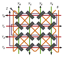
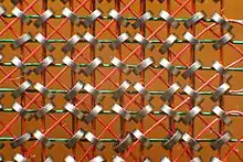
The term "core" comes from conventional transformers whose windings surround a magnetic core. In core memory, the wires pass once through any given core—they are single-turn devices. The properties of materials used for memory cores are dramatically different from those used in power transformers. The magnetic material for a core memory requires a high degree of magnetic remanence, the ability to stay highly magnetized, and a low coercivity so that less energy is required to change the magnetization direction. The core can take two states, encoding one bit. The core memory contents are retained even when the memory system is powered down (non-volatile memory). However, when the core is read, it is reset to a "zero" value. Circuits in the computer memory system then restore the information in an immediate re-write cycle.
How core memory works
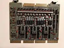
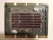
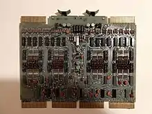
The most common form of core memory, X/Y line coincident-current, used for the main memory of a computer, consists of a large number of small toroidal ferrimagnetic ceramic ferrites (cores) held together in a grid structure (organized as a "stack" of layers called planes), with wires woven through the holes in the cores' centers. In early systems there were four wires: X, Y, Sense, and Inhibit, but later cores combined the latter two wires into one Sense/Inhibit line.[25] Each toroid stored one bit (0 or 1). One bit in each plane could be accessed in one cycle, so each machine word in an array of words was spread over a "stack" of planes. Each plane would manipulate one bit of a word in parallel, allowing the full word to be read or written in one cycle.
Core relies on the "square loop" properties of the ferrite material used to make the toroids. An electric current in a wire that passes through a core creates a magnetic field. Only a magnetic field greater than a certain intensity ("select") can cause the core to change its magnetic polarity. To select a memory location, one of the X and one of the Y lines are driven with half the current ("half-select") required to cause this change. Only the combined magnetic field generated where the X and Y lines cross (a logical AND function) is sufficient to change the state; other cores will see only half the needed field ("half-selected"), or none at all. By driving the current through the wires in a particular direction, the resulting induced field forces the selected core's magnetic flux to circulate in one direction or the other (clockwise or counterclockwise). One direction is a stored 1, while the other is a stored 0.
The toroidal shape of a core is preferred since the magnetic path is closed, there are no magnetic poles and thus very little external flux. This allows the cores to be packed closely together without allowing their magnetic fields to interact. The alternating 45-degree positioning used in early core arrays was necessitated by the diagonal sense wires. With the elimination of these diagonal wires, tighter packing was possible.[26]
Reading and writing
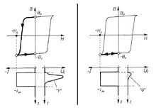
To read a bit of core memory, the circuitry tries to flip the bit to the polarity assigned to the 0 state, by driving the selected X and Y lines that intersect at that core.
- If the bit was already 0, the physical state of the core is unaffected.
- If the bit was previously 1, then the core changes magnetic polarity. This change, after a delay, induces a voltage pulse into the Sense line.
The detection of such a pulse means that the bit had most recently contained a 1. Absence of the pulse means that the bit had contained a 0. The delay in sensing the voltage pulse is called the access time of the core memory.
Following any such read, the bit contains a 0. This illustrates why a core memory access is called a destructive read: Any operation that reads the contents of a core erases those contents, and they must immediately be recreated.
To write a bit of core memory, the circuitry assumes there has been a read operation and the bit is in the 0 state.
- To write a 1 bit, the selected X and Y lines are driven, with current in the opposite direction as for the read operation. As with the read, the core at the intersection of the X and Y lines changes magnetic polarity.
- To write a 0 bit (in other words, to inhibit the writing of a 1 bit), the same amount of current is also sent through the Inhibit line. This reduces the net current flowing through the respective core to half the select current, inhibiting change of polarity.
The access time plus the time to rewrite is the memory cycle time.
The Sense wire is used only during the read, and the Inhibit wire is used only during the write. For this reason, later core systems combined the two into a single wire, and used circuitry in the memory controller to switch the function of the wire.
Core memory controllers were designed so that every read was followed immediately by a write (because the read forced all bits to 0, and because the write assumed this had happened). Computers began to take advantage of this fact. For example, a value in memory could be read and incremented (as for example by the AOS instruction on the PDP-6) almost as quickly as it could be read; the hardware simply incremented the value between the read phase and the write phase of a single memory cycle (perhaps signalling the memory controller to pause briefly in the middle of the cycle). This might be twice as fast as the process of obtaining the value with a read-write cycle, incrementing the value in some processor register, and then writing the new value with another read-write cycle.
Other forms of core memory
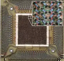
Word line core memory was often used to provide register memory. Other names for this type are linear select and 2-D. This form of core memory typically wove three wires through each core on the plane, word read, word write, and bit sense/write. To read or clear words, the full current is applied to one or more word read lines; this clears the selected cores and any that flip induce voltage pulses in their bit sense/write lines. For read, normally only one word read line would be selected; but for clear, multiple word read lines could be selected while the bit sense/write lines ignored. To write words, the half current is applied to one or more word write lines, and half current is applied to each bit sense/write line for a bit to be set. In some designs, the word read and word write lines were combined into a single wire, resulting in a memory array with just two wires per bit. For write, multiple word write lines could be selected. This offered a performance advantage over X/Y line coincident-current in that multiple words could be cleared or written with the same value in a single cycle. A typical machine's register set usually used only one small plane of this form of core memory. Some very large memories were built with this technology, for example the Extended Core Storage (ECS) auxiliary memory in the CDC 6600, which was up to 2 million 60-bit words.
Another form of core memory called core rope memory provided read-only storage. In this case, the cores, which had more linear magnetic materials, were simply used as transformers; no information was actually stored magnetically within the individual cores. Each bit of the word had one core. Reading the contents of a given memory address generated a pulse of current in a wire corresponding to that address. Each address wire was threaded either through a core to signify a binary [1], or around the outside of that core, to signify a binary [0]. As expected, the cores were much larger physically than those of read-write core memory. This type of memory was exceptionally reliable. An example was the Apollo Guidance Computer used for the NASA Moon landings.
Physical characteristics
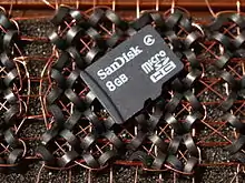
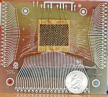
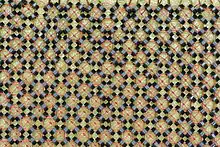

The performance of early core memories can be characterized in today's terms as being very roughly comparable to a clock rate of 1 MHz (equivalent to early 1980s home computers, like the Apple II and Commodore 64). Early core memory systems had cycle times of about 6 µs, which had fallen to 1.2 µs by the early 1970s, and by the mid-70s it was down to 600 ns (0.6 µs). Some designs had substantially higher performance: the CDC 6600 had a memory cycle time of 1.0 µs in 1964, using cores that required a half-select current of 200 mA.[33] Everything possible was done in order to decrease access times and increase data rates (bandwidth), including the simultaneous use of multiple grids of core, each storing one bit of a data word. For instance, a machine might use 32 grids of core with a single bit of the 32-bit word in each one, and the controller could access the entire 32-bit word in a single read/write cycle.
Core memory is non-volatile storage—it can retain its contents indefinitely without power. It is also relatively unaffected by EMP and radiation. These were important advantages for some applications like first-generation industrial programmable controllers, military installations and vehicles like fighter aircraft, as well as spacecraft, and led to core being used for a number of years after availability of semiconductor MOS memory (see also MOSFET). For example, the Space Shuttle IBM AP-101B flight computers used core memory, which preserved the contents of memory even through the Challenger's disintegration and subsequent plunge into the sea in 1986.[34] Another characteristic of early core was that the coercive force was very temperature-sensitive; the proper half-select current at one temperature is not the proper half-select current at another temperature. So a memory controller would include a temperature sensor (typically a thermistor) to adjust the current levels correctly for temperature changes. An example of this is the core memory used by Digital Equipment Corporation for their PDP-1 computer; this strategy continued through all of the follow-on core memory systems built by DEC for their PDP line of air-cooled computers. Another method of handling the temperature sensitivity was to enclose the magnetic core "stack" in a temperature controlled oven. Examples of this are the heated-air core memory of the IBM 1620 (which could take up to 30 minutes to reach operating temperature, about 106 °F (41 °C) and the heated-oil-bath core memory of the IBM 7090, early IBM 7094s, and IBM 7030.
Core was heated instead of cooled because the primary requirement was a consistent temperature, and it was easier (and cheaper) to maintain a constant temperature well above room temperature than one at or below it.
In 1980, the price of a 16 kW (kiloword, equivalent to 32 kB) core memory board that fitted into a DEC Q-bus computer was around US$3,000. At that time, core array and supporting electronics fit on a single printed circuit board about 25 × 20 cm in size, the core array was mounted a few mm above the PCB and was protected with a metal or plastic plate.
Diagnosing hardware problems in core memory required time-consuming diagnostic programs to be run. While a quick test checked if every bit could contain a one and a zero, these diagnostics tested the core memory with worst-case patterns and had to run for several hours. As most computers had just a single core memory board, these diagnostics also moved themselves around in memory, making it possible to test every bit. An advanced test was called a "Schmoo test" in which the half-select currents were modified along with the time at which the sense line was tested ("strobed"). The data plot of this test seemed to resemble a cartoon character called "Schmoo," and the name stuck. In many occasions, errors could be resolved by gently tapping the printed circuit board with the core array on a table. This slightly changed the positions of the cores along the wires running through them, and could fix the problem. The procedure was seldom needed, as core memory proved to be very reliable compared to other computer components of the day.
See also
References
- Bellis, Mary (23 February 2018). "Who Invented the Intel 1103 DRAM Chip?". Thought Co. US.
- Eckert, J. Presper (October 1953). "A Survey of Digital Computer Memory Systems". Proceedings of the IRE. US: IEEE. 41 (10): 1393–1406. doi:10.1109/JRPROC.1953.274316. ISSN 0096-8390.
- Reilly, Edwin D. (2003). Milestones in computer science and information technology. Westport, CT: Greenwood Press. p. 164. ISBN 1-57356-521-0.
- "Wang Interview, An Wang's Early Work in Core Memories". Datamation. US: Technical Publishing Company: 161–163. March 1976.
- US 2708722, Wang, An, "Pulse Transfer Controlling Device", issued 17 May 2020
- Forrester, Jay W. (1951). "Digital Information In Three Dimensions Using Magnetic Cores". Journal of Applied Physics (22). doi:10.1063/1.1699817.
- US 2736880, Forrester, Jay W., "Multicoordinate digital information storage device", issued 28 February 1956
- "Whirlwind" (PDF). The Computer Museum Report. Massachusetts: The Computer Museum: 13. Winter 1983 – via Microsoft.
- Evans, Christopher (July 1983). "Jay W. Forrester Interview". Annals of the History of Computing. 5 (3): 297–301. doi:10.1109/mahc.1983.10081.
- Kleiner, Art (4 February 2009). "Jay Forrester's Shock to the System". The MIT Sloan Review. US. Retrieved 1 April 2018.
- Jan A. Rajchman, Magnetic System, U.S. Patent 2,792,563, granted May. 14, 1957
- Hittinger, William (1992). "Jan A. Rajchman". Memorial Tributes. US: National Academy of Engineering. 5: 229.
- Redmond, Kent C.; Smith, Thomas M. (1980). Project Whirlwind - The History of a Pioneer Computer. Bedford, Mass.: Digital Press. p. 215. ISBN 0932376096.
- Commercially Available General Purpose Electronic Digital Computers of Moderate Price. Washington, D.C.: The Pentagon. 14 May 1952. Retrieved 16 February 2020.
- Pugh, Emerson W.; Johnson, Lyle R.; Palmer, John H. (1991). IBM's 360 and Early 370 Systems. US: MIT Press. p. 32. ISBN 978-0-262-51720-1.
- Clarence Schultz and George Boesen, Selectors for Automatic Phonographs, U.S. Patent 2,792,563, granted Feb. 2, 1960.
- "An Wang Sells Core Memory Patent to IBM". US: Computer History Museum. Retrieved 12 April 2010.
- "Magnetic Core Memory". CHM Revolution. Computer History Museum. Retrieved 1 April 2018.
- Pugh, Emerson W.; Johnson, Lyle R.; Palmer, John H. (1991). IBM's 360 and Early 370 Systems. Cambridge, MA: MIT Press. p. 182. ISBN 0-262-16123-0.
- Pugh, Emerson W.; Johnson, Lyle R.; Palmer, John H. (1991). IBM's 360 and Early 370 Systems. Cambridge, MA: MIT Press. pp. 204–206. ISBN 0-262-16123-0.
- Walter P. Shaw and Roderick W. Link, Method and Apparatus for Threading Perforated Articles, U.S. Patent 2,958,126, granted Nov. 1, 1960.
- Bashe, Charles J.; Johnson, Lyle R.; Palmer, John H. (1986). IBM's Early Computers. Cambridge, MA: MIT Press. p. 268. ISBN 0-262-52393-0.
- Robert L. Judge, Wire Threading Method and Apparatus, U.S. Patent 3,314,131, granted Apr. 18, 1967.
- Ronald A. Beck and Dennis L. Breu, Core Patch Stringing Method, U.S. Patent 3,872,581, granted Mar. 25, 1975.
- Creighton D. Barnes, et. al., Magnetic core storage device having a single winding for both the sensing and inhibit function, U.S. Patent 3,329,940, granted July 4, 1967.
- Victor L. Sell and Syed Alvi, High Density Core Memory Matrix, U.S. Patent 3,711,839, granted Jan. 16, 1973.
- Internally, the Moby Memory had 40 bits per word, but they were not exposed to the PDP-10 processor.
- Project MAC. Progress Report IV. July 1966-July 1967 (PDF) (Report). Massachusetts Institute of Technology. p. 18. 681342. Retrieved 7 December 2020.
- Eric S. Raymond, Guy L. Steele, The New Hacker's Dictionary, 3rd edition, 1996, ISBN 0262680920, based on the Jargon File, s.v. 'moby', p. 307
- "FABRI-TEK Mass Core 'Moby' Memory". Computer History Museum. US. 102731715. Retrieved 7 December 2020.
- Krakauer, Lawrence J. "Moby Memory". Retrieved 7 December 2020.
- Steven Levy, Hackers: Heroes of the Computer Revolution, 2010 (25th anniversary edition), ISBN 1449393748, p. 98
- "Section 4". Control Data 6600 Training Manual. Control Data Corporation. June 1965. Document number 60147400.
- "Magnetic Core Memory". US: National High Magnetic Field Laboratory: Museum of Electricity and Magnetism. Archived from the original on 10 June 2010.
Patents
- U.S. Patent 2,667,542 "Electric connecting device" (matrix switch with iron cores that operate as a cross-point switch. A series of X analog or telephone signal inputs can be routed to Y outputs.), filed September 1951, issued January 1954
- U.S. Patent 2,708,722 "Pulse transfer controlling devices", An Wang filed October 1949, issued May 1955
- U.S. Patent 2,736,880 "Multicoordinate digital information storage device" (coincident-current system), Jay Forrester filed May 1951, issued February 28, 1956
- U.S. Patent 2,970,291 "Electronic Relay Circuit" (The patent notes "My invention relates to electric circuits employing relays...") filed May 28, 1947, issued January 31, 1961.
- U.S. Patent 2,992,414 "Memory Transformer" (The patent notes that "My invention relates to electric relay circuits and more particularly to improved transformers for use therein.") filed May 29, 1947, issued July 11, 1961.
- U.S. Patent 3,161,861 "Magnetic core memory" (improvements) Ken Olsen filed November 1959, issued December 1964
- U.S. Patent 3,264,713 "Method of Making Memory Core Structures" (The patent notes "This invention relates to magnetic memory devices, and more particularly to a new and improved memory core structure and method of making the same...") filed January 30, 1962, issued August 9, 1966.
- U.S. Patent 3,421,152 "Linear select magnetic memory system and controls therefor", W. J. Mahoney, issued January 7, 1969
- U.S. Patent 4,161,037 "Ferrite core memory" (automated production), July 1979
- U.S. Patent 4,464,752 "Multiple event hardened core memory" (radiation protection), August, 1984
External links
| Wikimedia Commons has media related to Core memory. |
| Look up core memory in Wiktionary, the free dictionary. |
- Interactive Java Tutorial - Magnetic Core Memory National High Magnetic Field Laboratory
- Core Memory at Columbia University
- Navy Manual
- Core Memory on the PDP-11
- Core memory and other early memory types accessed April 15, 2006
- Coincident Current Ferrite Core Memories Byte magazine, July 1976
- Casio AL-1000 calculator – Shows close-ups of the magnetic core memory in this desktop electronic calculator from the mid-1960s.
- Still used core memory in multiple devices in a German computer museum
- A 110-Nanosecond Ferrite Core Memory
- background on core memory for computers
