Thin-film transistor
A thin-film transistor (TFT) is a special type of metal–oxide–semiconductor field-effect transistor (MOSFET)[1] made by depositing thin films of an active semiconductor layer as well as the dielectric layer and metallic contacts over a supporting (but non-conducting) substrate. A common substrate is glass, because the primary application of TFTs is in liquid-crystal displays (LCDs). This differs from the conventional bulk MOSFET transistor,[1] where the semiconductor material typically is the substrate, such as a silicon wafer.
Manufacture
TFTs can be made using a wide variety of semiconductor materials. A common material is silicon. The characteristics of a silicon-based TFT depend on the silicon's crystalline state; that is, the semiconductor layer can be either amorphous silicon,[2] microcrystalline silicon,[2] or it can be annealed into polysilicon.
Other materials which have been used as semiconductors in TFTs include compound semiconductors such as cadmium selenide,[3][4] or metal oxides such as zinc oxide[5] or hafnium oxide. An application for hafnium oxide is as a high-κ dielectric.[6] TFTs have also been made using organic materials, referred to as organic field-effect transistors or OTFTs.
By using transparent semiconductors and transparent electrodes, such as indium tin oxide (ITO), some TFT devices can be made completely transparent. Such transparent TFTs (TTFTs) can be used for construction of video display panels. Because conventional substrates cannot withstand high annealing temperatures, the deposition process must be completed under relatively low temperatures. Chemical vapor deposition and physical vapor deposition (usually sputtering) are applied. The first solution-processed TTFTs, based on zinc oxide, were reported in 2003 by researchers at Oregon State University.[5] The Portuguese laboratory CENIMAT at the Universidade Nova de Lisboa has produced the world's first completely transparent TFT at room temperature.[7] CENIMAT also developed the first paper transistor,[8] which may lead to applications such as magazines and journal pages with moving images.
During production, TFTs are repaired using Lasers, ink dispensers and Chemical Vapor Deposition (CVD).[9]
Applications
The best known application of thin-film transistors is in TFT LCDs, an implementation of liquid-crystal display technology. Transistors are embedded within the panel itself, reducing crosstalk between pixels and improving image stability.
As of 2008, many color LCD TVs and monitors use this technology. TFT panels are frequently used in digital radiography applications in general radiography. A TFT is used in both direct and indirect capture as a base for the image receptor in medical radiography.
As of 2013, all modern high-resolution and high-quality electronic visual display devices use TFT-based active matrix displays.[10]
AMOLED displays also contain a TFT layer for active-matrix pixel addressing of individual organic light-emitting diodes.
The most beneficial aspect of TFT technology is its use of a separate transistor for each pixel on the display. Because each transistor is small, the amount of charge needed to control it is also small. This allows for very fast re-drawing of the display.
Structure of a TFT-display matrix
This picture does not include the actual light-source (usually cold-cathode fluorescent lamps or white LEDs), just the TFT-display matrix.
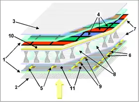 Cut through an TFT display.
|
|
History
In February 1957, John Wallmark of RCA filed a patent for a thin film MOSFET in which germanium monoxide was used as a gate dielectric. Paul K. Weimer, also of RCA implemented Wallmark's ideas and developed the thin-film transistor (TFT) in 1962, a type of MOSFET distinct from the standard bulk MOSFET. It was made with thin films of cadmium selenide and cadmium selenide. In 1966, T.P. Brody and H.E. Kunig at Westinghouse Electric fabricated indium arsenide (InAs) MOS TFTs in both depletion and enhancement modes.[11][12][13][14][1][15][16]
The idea of a TFT-based liquid-crystal display (LCD) was conceived by Bernard J. Lechner of RCA Laboratories in 1968.[17] Lechner, F.J. Marlowe, E.O. Nester and J. Tults demonstrated the concept in 1968 with an 18x2 matrix dynamic scattering LCD that used standard discrete MOSFETs, as TFT performance was not adequate at the time.[18] In 1973, T. Peter Brody, J. A. Asars and G. D. Dixon at Westinghouse Research Laboratories developed a CdSe (cadmium selenide) TFT, which they used to demonstrate the first CdSe thin-film-transistor liquid-crystal display (TFT LCD).[14][19] The Westinghouse group also reported on operational TFT electroluminescence (EL) in 1973, using CdSe.[20] Brody and Fang-Chen Luo demonstrated the first flat active-matrix liquid-crystal display (AM LCD) using CdSe in 1974, and then Brody coined the term "active matrix" in 1975.[17] However, mass production of this device was never realized, due to complications in controlling the compound semiconductor thin film material properties, and device reliability over large areas.[14]
A breakthrough in TFT research came with the development of the amorphous silicon (a-Si) TFT by P.G. le Comber, W.E. Spear and A. Ghaith at the University of Dundee in 1979. They reported the first functional TFT made from hydrogenated a-Si with a silicon nitride gate dielectric layer.[14][21] The a-Si TFT was soon recognized as being more suitable for a large-area AM LCD.[14] This led to commercial research and development (R&D) of AM LCD panels based on a-Si TFTs in Japan.[22]
By 1982, pocket LCD TVs based on AM LCD technology were developed in Japan.[23] In 1982, Fujitsu's S. Kawai fabricated an a-Si dot-matrix display, and Canon's Y. Okubo fabricated a-Si twisted nematic (TN) and guest-host LCD panels. In 1983, Toshiba's K. Suzuki produced a-Si TFT arrays compatible with CMOS integrated circuits (ICs), Canon's M. Sugata fabricated an a-Si color LCD panel, and a joint Sanyo and Sanritsu team including Mitsuhiro Yamasaki, S. Suhibuchi and Y. Sasaki fabricated a 3-inch a-SI color LCD TV.[22]
The first commercial TFT-based AM LCD product was the 2.1-inch Epson ET-10[20] (Epson Elf), the first color LCD pocket TV, released in 1984.[24] In 1986, a Hitachi research team led by Akio Mimura demonstrated a low-temperature polycrystalline silicon (LTPS) process for fabricating n-channel TFTs on a silicon-on-insulator (SOI), at a relatively low temperature of 200°C.[25] A Hosiden research team led by T. Sunata in 1986 used a-Si TFTs to develop a 7-inch color AM LCD panel,[26] and a 9-inch AM LCD panel.[27] In the late 1980s, Hosiden supplied monochrome TFT LCD panels to Apple Computers.[14] In 1988, a Sharp research team led by engineer T. Nagayasu used hydrogenated a-Si TFTs to demonstrate a 14-inch full-color LCD display,[17][28] which convinced the electronics industry that LCD would eventually replace cathode-ray tube (CRT) as the standard television display technology.[17] The same year, Sharp launched TFT LCD panels for notebook PCs.[20] In 1992, Toshiba and IBM Japan introduced a 12.1-inch color SVGA panel for the first commercial color laptop by IBM.[20]
TFTs can also be made out of indium gallium zinc oxide (IGZO) TFT-LCDs with IGZO transistors first showed up in 2012, and were first manufactured by Sharp Corporation. IGZO allows for higher refresh rates and lower power consumption.[29][30]
References
- Kimizuka, Noboru; Yamazaki, Shunpei (2016). Physics and Technology of Crystalline Oxide Semiconductor CAAC-IGZO: Fundamentals. John Wiley & Sons. p. 217. ISBN 9781119247401.
- Kanicki, Jerzy (1992). Amorphous & Microcystalline Semiconductor Devices Volume II: Materials and Device Physics. Artech House, Inc. ISBN 0-89006-379-6.
- Brody, T. Peter (November 1984). "The Thin Film Transistor - A Late Flowering Bloom". IEEE Transactions on Electron Devices. 31 (11): 1614–1628. doi:10.1109/T-ED.1984.21762.
- Brody, T. Peter (1996). "The birth and early childhood of active matrix - a personal memoir". Journal of the SID. 4/3: 113–127.
- Wager, John. OSU Engineers Create World's First Transparent Transistor Archived 2007-09-15 at the Wayback Machine. College of Engineering, Oregon State University, Corvallis, OR: OSU News & Communication, 2003. 29 July 2007.
- Chun, Yoon Soo; Chang, Seongpil; Lee, Sang Yeol (2011). "Effects of gate insulators on the performance of a-IGZO TFT fabricated at room-temperature". Microelectronic Engineering. 88 (7): 1590–1593. doi:10.1016/j.mee.2011.01.076. ISSN 0167-9317.
- Fortunato, E. M. C.; Barquinha, P. M. C.; Pimentel, A. C. M. B. G.; Gonçalves, A. M. F.; Marques, A. J. S.; Pereira, L. M. N.; Martins, R. F. P. (March 2005). "Fully Transparent ZnO Thin-Film Transistor Produced at Room Temperature". Advanced Materials. 17 (5): 590–594. doi:10.1002/adma.200400368.
- Fortunato, E.; Correia, N.; Barquinha, P.; Pereira, L.; Goncalves, G.; Martins, R. (September 2008). "High-Performance Flexible Hybrid Field-Effect Transistors Based on Cellulose Fiber Paper" (PDF). IEEE Electron Device Letters. 29 (9): 988–990. doi:10.1109/LED.2008.2001549.
- "V-TECHNOLOGY CO., LTD. - FPD Inspection | Products and Services | V-TECHNOLOGY CO., LTD". www.vtec.co.jp.
- Brotherton, S. D. (2013). Introduction to Thin Film Transistors: Physics and Technology of TFTs. Springer Science & Business Media. p. 74. ISBN 9783319000022.
- Woodall, Jerry M. (2010). Fundamentals of III-V Semiconductor MOSFETs. Springer Science & Business Media. pp. 2–3. ISBN 9781441915474.
- Brody, T. P.; Kunig, H. E. (October 1966). "A HIGH‐GAIN InAs THIN‐FILM TRANSISTOR". Applied Physics Letters. 9 (7): 259–260. doi:10.1063/1.1754740. ISSN 0003-6951.
- Weimer, Paul K. (June 1962). "The TFT A New Thin-Film Transistor". Proceedings of the IRE. 50 (6): 1462–1469. doi:10.1109/JRPROC.1962.288190. ISSN 0096-8390.
- Kuo, Yue (1 January 2013). "Thin Film Transistor Technology—Past, Present, and Future" (PDF). The Electrochemical Society Interface. 22 (1): 55–61. doi:10.1149/2.F06131if. ISSN 1064-8208.
- Lojek, Bo (2007). History of Semiconductor Engineering. Springer Science & Business Media. pp. 322–324. ISBN 978-3540342588.
- Richard Ahrons (2012). "Industrial Research in Microcircuitry at RCA: The Early Years, 1953–1963". 12 (1). IEEE Annals of the History of Computing: 60–73. Cite journal requires
|journal=(help) - Kawamoto, H. (2012). "The Inventors of TFT Active-Matrix LCD Receive the 2011 IEEE Nishizawa Medal". Journal of Display Technology. 8 (1): 3–4. doi:10.1109/JDT.2011.2177740. ISSN 1551-319X.
- Castellano, Joseph A. (2005). Liquid Gold: The Story of Liquid Crystal Displays and the Creation of an Industry. World Scientific. pp. 41–2. ISBN 9789812389565.
- Brody, T. Peter; Asars, J. A.; Dixon, G. D. (November 1973). "A 6 × 6 inch 20 lines-per-inch liquid-crystal display panel". IEEE Transactions on Electron Devices. 20 (11): 995–1001. doi:10.1109/T-ED.1973.17780. ISSN 0018-9383.
- Souk, Jun; Morozumi, Shinji; Luo, Fang-Chen; Bita, Ion (2018). Flat Panel Display Manufacturing. John Wiley & Sons. pp. 2–3. ISBN 9781119161356.
- Comber, P. G. le; Spear, W. E.; Ghaith, A. (1979). "Amorphous-silicon field-effect device and possible application". Electronics Letters. 15 (6): 179–181. doi:10.1049/el:19790126. ISSN 0013-5194.
- Castellano, Joseph A. (2005). Liquid Gold: The Story of Liquid Crystal Displays and the Creation of an Industry. World Scientific. pp. 180, 181, 188. ISBN 9789812565846.
- Morozumi, Shinji; Oguchi, Kouichi (12 October 1982). "Current Status of LCD-TV Development in Japan". Molecular Crystals and Liquid Crystals. 94 (1–2): 43–59. doi:10.1080/00268948308084246. ISSN 0026-8941.
- "ET-10". Epson. Retrieved 29 July 2019.
- Mimura, Akio; Oohayashi, M.; Ohue, M.; Ohwada, J.; Hosokawa, Y. (1986). "SOI TFT's with directly contacted ITO". IEEE Electron Device Letters. 7 (2): 134–136. doi:10.1109/EDL.1986.26319. ISSN 0741-3106.
- Sunata, T.; Yukawa, T.; Miyake, K.; Matsushita, Y.; Murakami, Y.; Ugai, Y.; Tamamura, J.; Aoki, S. (1986). "A large-area high-resolution active-matrix color LCD addressed by a-Si TFT's". IEEE Transactions on Electron Devices. 33 (8): 1212–1217. doi:10.1109/T-ED.1986.22644. ISSN 0018-9383.
- Sunata, T.; Miyake, K.; Yasui, M.; Murakami, Y.; Ugai, Y.; Tamamura, J.; Aoki, S. (1986). "A 640 × 400 pixel active-matrix LCD using a-Si TFT's". IEEE Transactions on Electron Devices. 33 (8): 1218–1221. doi:10.1109/T-ED.1986.22645. ISSN 0018-9383.
- Nagayasu, T.; Oketani, T.; Hirobe, T.; Kato, H.; Mizushima, S.; Take, H.; Yano, K.; Hijikigawa, M.; Washizuka, I. (October 1988). "A 14-in.-diagonal full-color a-Si TFT LCD". Conference Record of the 1988 International Display Research Conference: 56–58. doi:10.1109/DISPL.1988.11274.
- Orland, Kyle (August 8, 2019). "What Sharp's IGZO display technology will mean for the Nintendo Switch". Ars Technica.
- "IGZO Display Technology - Sharp". www.sharpsma.com.