Multigate device
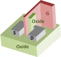
A multigate device, multi-gate MOSFET or multi-gate field-effect transistor (MuGFET) refers to a metal–oxide–semiconductor field-effect transistor (MOSFET) that incorporates more than one gate into a single device. The multiple gates may be controlled by a single gate electrode, wherein the multiple gate surfaces act electrically as a single gate, or by independent gate electrodes. A multigate device employing independent gate electrodes is sometimes called a multiple-independent-gate field-effect transistor (MIGFET). The most widely used multi-gate devices are the FinFET (fin field-effect transistor) and the GAAFET (gate-all-around field-effect transistor), which are non-planar transistors, or 3D transistors.
Multi-gate transistors are one of the several strategies being developed by MOS semiconductor manufacturers to create ever-smaller microprocessors and memory cells, colloquially referred to as extending Moore's law (in its narrow, specific version concerning density scaling, exclusive of its careless historical conflation with Dennard scaling).[1] Development efforts into multigate transistors have been reported by the Electrotechnical Laboratory, Toshiba, Grenoble INP, Hitachi, IBM, TSMC, UC Berkeley, Infineon Technologies, Intel, AMD, Samsung Electronics, KAIST, Freescale Semiconductor, and others, and the ITRS predicted correctly that such devices will be the cornerstone of sub-32 nm technologies.[2] The primary roadblock to widespread implementation is manufacturability, as both planar and non-planar designs present significant challenges, especially with respect to lithography and patterning. Other complementary strategies for device scaling include channel strain engineering, silicon-on-insulator-based technologies, and high-κ/metal gate materials.
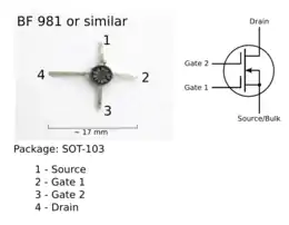
Dual-gate MOSFETs are commonly used in very high frequency (VHF) mixers and in sensitive VHF front-end amplifiers. They are available from manufacturers such as Motorola, NXP Semiconductors, and Hitachi.[3][4][5]
Types
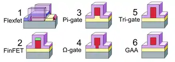
Dozens of multigate transistor variants may be found in the literature. In general, these variants may be differentiated and classified in terms of architecture (planar vs. non-planar design) and the number of channels/gates (2, 3, or 4).
Planar double-gate MOSFET (DGMOS)
A planar double-gate MOSFET (DGMOS) employs conventional planar (layer-by-layer) manufacturing processes to create double-gate MOSFET (metal-oxide-semiconductor field-effect transistor) devices, avoiding more stringent lithography requirements associated with non-planar, vertical transistor structures. In planar double-gate transistors the drain–source channel is sandwiched between two independently fabricated gate/gate-oxide stacks. The primary challenge in fabricating such structures is achieving satisfactory self-alignment between the upper and lower gates.[6]
After the MOSFET was first demonstrated by Mohamed Atalla and Dawon Kahng of Bell Labs in 1960,[7] the concept of a double-gate thin-film transistor (TFT) was proposed by H.R. Farrah (Bendix Corporation) and R.F. Steinberg in 1967.[8] The concept of a double-gate MOSFET was later proposed by Toshihiro Sekigawa of the Electrotechnical Laboratory (ETL) in a 1980 patent describing the planar XMOS transistor.[9] Sekigawa fabricated the XMOS transistor with Yutaka Hayashi at the ETL in 1984. They demonstrated that short-channel effects can be significantly reduced by sandwiching a fully depleted silicon-on-insulator (SOI) device between two gate electrodes connected together.[10][11]
The ETL demonstration inspired Grenoble INP researchers including Francis Balestra, Sorin Cristoloveanu, M. Benachir and Tarek Elewa to fabricate a double-gate MOSFET using silicon thin film in 1987. The double-gate control of SOI transistors was used to force the whole silicon film (interface layers and volume) in strong inversion (called “Volume-Inversion MOSFET”) or strong accumulation (called “Volume-Accumulation MOSFET”). This method of transistor operation, demonstrating the electrostatic properties and scalability of multigate devices, offered strong device performance, particularly substantial increases in subthreshold slope, transconductance, and drain current. A simulation program and experiments on SIMOX structures was used to study this device.[12]
Sekigawa fabricated an XMOS device with 2 µm gate length in 1987.[9] In 1988, an IBM research team led by Bijan Davari fabricated 180 nm to 250 nm dual-gate CMOS devices.[13][14] In 1992, Sekigawa fabricated a 380 nm XMOS device. In 1998, E. Suzuki fabricated a 40 nm XMOS device. The focus of DGMOS research and development (R&D) subsequently shifted away from planar DGMOS technology, towards non-planar FinFET (fin field-effect transistor) and GAAFET (gate-all-around field-effect transistor) technologies.[9]
FlexFET
FlexFET is a planar, independently double-gated transistor with a damascene metal top gate MOSFET and an implanted JFET bottom gate that are self-aligned in a gate trench. This device is highly scalable due to its sub-lithographic channel length; non-implanted ultra-shallow source and drain extensions; non-epi raised source and drain regions; and gate-last flow. FlexFET is a true double-gate transistor in that (1) both the top and bottom gates provide transistor operation, and (2) the operation of the gates is coupled such that the top gate operation affects the bottom gate operation and vice versa.[15] Flexfet was developed and is manufactured by American Semiconductor, Inc.
FinFET
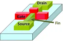
FinFET (fin field-effect transistor) is a type of non-planar transistor, or "3D" transistor (not to be confused with 3D microchips).[16] The FinFET is a variation on traditional MOSFETs distinguished by the presence of a thin silicon "fin" inversion channel on top of the substrate, allowing the gate to make two points of contact: the left and right sides of the fin. The thickness of the fin (measured in the direction from source to drain) determines the effective channel length of the device. The wrap-around gate structure provides a better electrical control over the channel and thus helps in reducing the leakage current and overcoming other short-channel effects.
The first finfet transistor type was called a "Depleted Lean-channel Transistor" or "DELTA" transistor, which was first fabricated by Hitachi Central Research Laboratory's Digh Hisamoto, Toru Kaga, Yoshifumi Kawamoto and Eiji Takeda in 1989.[17][10][18] In the late 1990s, Digh Hisamoto began collaborating with an international team of researchers on further developing DELTA technology, including TSMC's Chenming Hu and a UC Berkeley research team including Tsu-Jae King Liu, Jeffrey Bokor, Xuejue Huang, Leland Chang, Nick Lindert, S. Ahmed, Cyrus Tabery, Yang‐Kyu Choi, Pushkar Ranade, Sriram Balasubramanian, A. Agarwal and M. Ameen. In 1998, the team developed the first N-channel FinFETs and successfully fabricated devices down to a 17 nm process. The following year, they developed the first P-channel FinFETs.[19] They coined the term "FinFET" (fin field-effect transistor) in a December 2000 paper.[20]
In current usage the term FinFET has a less precise definition. Among microprocessor manufacturers, AMD, IBM, and Freescale describe their double-gate development efforts as FinFET[21] development, whereas Intel avoids using the term when describing their closely related tri-gate architecture.[22] In the technical literature, FinFET is used somewhat generically to describe any fin-based, multigate transistor architecture regardless of number of gates. It is common for a single FinFET transistor to contain several fins, arranged side by side and all covered by the same gate, that act electrically as one, to increase drive strength and performance.[23] The gate may also cover the entirety of the fin(s).
A 25 nm transistor operating on just 0.7 volt was demonstrated in December 2002 by TSMC (Taiwan Semiconductor Manufacturing Company). The "Omega FinFET" design is named after the similarity between the Greek letter omega (Ω) and the shape in which the gate wraps around the source/drain structure. It has a gate delay of just 0.39 picosecond (ps) for the N-type transistor and 0.88 ps for the P-type.
In 2004, Samsung Electronics demonstrated a "Bulk FinFET" design, which made it possible to mass-produce FinFET devices. They demonstrated dynamic random-access memory (DRAM) manufactured with a 90 nm Bulk FinFET process.[19] In 2006, a team of Korean researchers from the Korea Advanced Institute of Science and Technology (KAIST) and the National Nano Fab Center developed a 3 nm transistor, the world's smallest nanoelectronic device, based on FinFET technology.[24][25] In 2011, Rice University researchers Masoud Rostami and Kartik Mohanram demonstrated that FINFETs can have two electrically independent gates, which gives circuit designers more flexibility to design with efficient, low-power gates.[26]
In 2012, Intel started using FinFETs for its future commercial devices. Leaks suggest that Intel's FinFET has an unusual shape of a triangle rather than rectangle, and it is speculated that this might be either because a triangle has a higher structural strength and can be more reliably manufactured or because a triangular prism has a higher area-to-volume ratio than a rectangular prism, thus increasing switching performance.[27]
In September 2012, GlobalFoundries announced plans to offer a 14-nanometer process technology featuring FinFET three-dimensional transistors in 2014.[28] The next month, the rival company TSMC announced start early or "risk" production of 16 nm FinFETS in November 2013.[29]
In March 2014, TSMC announced that it is nearing implementation of several 16 nm FinFETs die-on wafers manufacturing processes:[30]
- 16 nm FinFET (Q4 2014),
- 16 nm FinFET+ (cca Q4 2014),
- 16 nm FinFET "Turbo" (estimated in 2015–2016).
AMD released GPUs using their Polaris chip architecture and made on 14 nm FinFET in June 2016.[31] The company has tried to produce a design to provide a "generational jump in power efficiency" while also offering stable frame rates for graphics, gaming, virtual reality, and multimedia applications.[32]
In March 2017, Samsung and eSilicon announced the tapeout for production of a 14 nm FinFET ASIC in a 2.5D package.[33][34]
Tri-gate transistor
A tri-gate transistor, also known as a triple-gate transistor, is a type of MOSFET with a gate on three of its sides.[35] A triple-gate transistor was first demonstrated in 1987, by a Toshiba research team including K. Hieda, Fumio Horiguchi and H. Watanabe. They realized that the fully depleted (FD) body of a narrow bulk Si-based transistor helped improve switching due to a lessened body-bias effect.[36][37] In 1992, a triple-gate MOSFET was demonstrated by IBM researcher Hon-Sum Wong.[38]
Tri-gate fabrication is used by Intel for the non-planar transistor architecture used in Ivy Bridge, Haswell and Skylake processors. These transistors employ a single gate stacked on top of two vertical gates (a single gate wrapped over three sides of the channel), allowing essentially three times the surface area for electrons to travel. Intel reports that their tri-gate transistors reduce leakage and consume far less power than current transistors. This allows up to 37% higher speed or a power consumption at under 50% of the previous type of transistors used by Intel.[39][40]
Intel explains: "The additional control enables as much transistor current flowing as possible when the transistor is in the 'on' state (for performance), and as close to zero as possible when it is in the 'off' state (to minimize power), and enables the transistor to switch very quickly between the two states (again, for performance)."[41] Intel has stated that all products after Sandy Bridge will be based upon this design.
Intel announced this technology in September 2002.[42] Intel announced "triple-gate transistors" which maximize "transistor switching performance and decreases power-wasting leakage". A year later, in September 2003, AMD announced that it was working on similar technology at the International Conference on Solid State Devices and Materials.[43][44] No further announcements of this technology were made until Intel's announcement in May 2011, although it was stated at IDF 2011, that they demonstrated a working SRAM chip based on this technology at IDF 2009.[45]
On April 23, 2012, Intel released a new line of CPUs, termed Ivy Bridge, which feature tri-gate transistors.[46][47] Intel has been working on its tri-gate architecture since 2002, but it took until 2011 to work out mass-production issues. The new style of transistor was described on May 4, 2011, in San Francisco.[48] Intel factories are expected to make upgrades over 2011 and 2012 to be able to manufacture the Ivy Bridge CPUs.[49] As well as being used in Intel's Ivy Bridge chips for desktop PCs, the new transistors will also be used in Intel's Atom chips for low-powered devices.[48]
The term tri-gate is sometimes used generically to denote any multigate FET with three effective gates or channels.
Gate-all-around FET (GAAFET)
A gate-all-around (GAA) FET, abbreviated GAAFET, and also known as a surrounding-gate transistor (SGT),[50][51] is similar in concept to a FinFET except that the gate material surrounds the channel region on all sides. Depending on design, gate-all-around FETs can have two or four effective gates. Gate-all-around FETs have been successfully characterized both theoretically and experimentally.[52][53] They have also been successfully etched onto InGaAs nanowires, which have a higher electron mobility than silicon.[54] GAAFETs are the successor to FinFETs, as they can work at sizes below 7 nm. They were used by IBM to demonstrate 5 nm process technology.
A gate-all-around (GAA) MOSFET was first demonstrated in 1988, by a Toshiba research team including Fujio Masuoka, Hiroshi Takato, and Kazumasa Sunouchi, who demonstrated a vertical nanowire GAAFET which they called a "surrounding gate transistor" (SGT).[55][56][51] Masuoka, best known as the inventor of flash memory, later left Toshiba and founded Unisantis Electronics in 2004 to research surrounding-gate technology along with Tohoku University.[57] In 2006, a team of Korean researchers from the Korea Advanced Institute of Science and Technology (KAIST) and the National Nano Fab Center developed a 3 nm transistor, the world's smallest nanoelectronic device, based on gate-all-around (GAA) FinFET technology.[58][25]
As of 2020, Samsung and Intel have announced plans to mass produce GAAFET transistors (specifically MBCFET transistors) while TSMC has announced that they will continue to use FinFETs in their 3nm node,[59] despite TSMC developing GAAFET transistors.[60]
Multi-bridge channel (MBC) FET
A multi-bridge channel FET (MBCFET) is similar to a GAAFET except for the use of nanosheets instead of nanowires.[61] MBCFET is a word mark (trademark) registered in the U.S. to Samsung Electronics.[62] Samsung plans on mass producing MBCFET transistors at the 3 nm node for its foundry customers.[63] Intel is also developing MBCFET "nanoribbon" transistors.[64]
Industry need
Planar transistors have been the core of integrated circuits for several decades, during which the size of the individual transistors has steadily decreased. As the size decreases, planar transistors increasingly suffer from the undesirable short-channel effect, especially "off-state" leakage current, which increases the idle power required by the device.[65]
In a multigate device, the channel is surrounded by several gates on multiple surfaces. Thus it provides better electrical control over the channel, allowing more effective suppression of "off-state" leakage current. Multiple gates also allow enhanced current in the "on" state, also known as drive current. Multigate transistors also provide a better analog performance due to a higher intrinsic gain and lower channel length modulation.[66] These advantages translate to lower power consumption and enhanced device performance. Nonplanar devices are also more compact than conventional planar transistors, enabling higher transistor density which translates to smaller overall microelectronics.
Integration challenges
The primary challenges to integrating nonplanar multigate devices into conventional semiconductor manufacturing processes include:
- Fabrication of a thin silicon "fin" tens of nanometers wide
- Fabrication of matched gates on multiple sides of the fin
Compact modeling

BSIMCMG106.0.0,[67] officially released on March 1, 2012 by UC Berkeley BSIM Group, is the first standard model for FinFETs. BSIM-CMG is implemented in Verilog-A. Physical surface-potential-based formulations are derived for both intrinsic and extrinsic models with finite body doping. The surface potentials at the source and drain ends are solved analytically with poly-depletion and quantum mechanical effects. The effect of finite body doping is captured through a perturbation approach. The analytic surface potential solution agrees closely with the 2-D device simulation results. If the channel doping concentration is low enough to be neglected, computational efficiency can be further improved by a setting a specific flag (COREMOD = 1).
All of the important multi-gate (MG) transistor behavior is captured by this model. Volume inversion is included in the solution of Poisson's equation, hence the subsequent I–V formulation automatically captures the volume-inversion effect. Analysis of electrostatic potential in the body of MG MOSFETs provided a model equation for short-channel effects (SCE). The extra electrostatic control from the end gates (top/bottom gates) (triple or quadruple-gate) is also captured in the short-channel model.
See also
- Three-dimensional integrated circuit
- Semiconductor device
- Clock gating
- High-κ dielectric
- Next-generation lithography
- Extreme ultraviolet lithography
- Immersion lithography
- Strain engineering
- Very-large-scale integration (VLSI)
- Neuromorphic engineering
- Bit slicing
- 3D printing
- Silicon on insulator (SOI)
- MOSFET
- Floating-gate MOSFET
- Transistor
- BSIM
- High electron mobility transistor
- Field-effect transistor
- JFET
- Tetrode transistor
- Pentode transistor
- Memristor
- Quantum circuit
- Quantum gate
- Transistor model
- Die shrink
References
- Risch, L. "Pushing CMOS Beyond the Roadmap", Proceedings of ESSCIRC, 2005, p. 63.
- Table39b Archived September 27, 2007, at the Wayback Machine
- "3N201 (Motorola) - Dual Gate Mosfet Vhf Amplifier". Doc.chipfind.ru. Retrieved 2014-03-10.
- "3SK45 datasheet pdf datenblatt - Hitachi Semiconductor - SILICON N-CHANNEL DUAL GATE MOSFET". Alldatasheet.com. Retrieved 2014-03-10.
- "BF1217WR" (PDF). Retrieved 2015-05-10.
- Wong, H-S.; Chan, K.; Taur, Y. (December 10, 1997). Self-aligned (top and bottom) double-gate MOSFET with a 25 nm thick silicon channel. Electron Devices Meeting, 1997. IEDM '97. Technical Digest. pp. 427–430. doi:10.1109/IEDM.1997.650416. ISBN 978-0-7803-4100-5. ISSN 0163-1918. S2CID 20947344.
- "1960: Metal Oxide Semiconductor (MOS) Transistor Demonstrated". The Silicon Engine. Computer History Museum. Retrieved 25 September 2019.
- Farrah, H.R.; Steinberg, R.F. (February 1967). "Analysis of double-gate thin-film transistor". IEEE Transactions on Electron Devices. 14 (2): 69–74. Bibcode:1967ITED...14...69F. doi:10.1109/T-ED.1967.15901.
- Koike, Hanpei; Nakagawa, Tadashi; Sekigawa, Toshiro; Suzuki, E.; Tsutsumi, Toshiyuki (23 February 2003). "Primary Consideration on Compact Modeling of DG MOSFETs with Four-terminal Operation Mode" (PDF). TechConnect Briefs. 2 (2003): 330–333. S2CID 189033174.
- Colinge, J.P. (2008). FinFETs and Other Multi-Gate Transistors. Springer Science & Business Media. pp. 11 & 39. ISBN 9780387717517.
- Sekigawa, Toshihiro; Hayashi, Yutaka (August 1984). "Calculated threshold-voltage characteristics of an XMOS transistor having an additional bottom gate". Solid-State Electronics. 27 (8): 827–828. Bibcode:1984SSEle..27..827S. doi:10.1016/0038-1101(84)90036-4. ISSN 0038-1101.
- Balestra, Francis; Cristoloveanu, Sorin; Benachir, M.; Elewa, Tarek; Brini, Jean (September 1987). "Double-gate silicon-on-insulator transistor with volume inversion: A new device with greatly enhanced performance". IEEE Electron Device Letters. 8 (9): 410–412. Bibcode:1987IEDL....8..410B. doi:10.1109/EDL.1987.26677. ISSN 0741-3106. S2CID 39090047.
- Davari, Bijan; Chang, Wen-Hsing; Wordeman, Matthew R.; Oh, C. S.; Taur, Yuan; Petrillo, Karen E.; Rodriguez, M. D. (December 1988). "A high performance 0.25 mu m CMOS technology". Technical Digest., International Electron Devices Meeting: 56–59. doi:10.1109/IEDM.1988.32749. S2CID 114078857.
- Davari, Bijan; Wong, C. Y.; Sun, Jack Yuan-Chen; Taur, Yuan (December 1988). "Doping of n/sup +/ and p/sup +/ polysilicon in a dual-gate CMOS process". Technical Digest., International Electron Devices Meeting: 238–241. doi:10.1109/IEDM.1988.32800. S2CID 113918637.
- Wilson, D.; Hayhurst, R.; Oblea, A.; Parke, S.; Hackler, D. "Flexfet: Independently-Double-Gated SOI Transistor With Variable Vt and 0.5V Operation Achieving Near Ideal Subthreshold Slope" SOI Conference, 2007 IEEE International Archived April 3, 2015, at the Wayback Machine
- "What is Finfet?". Computer Hope. April 26, 2017. Retrieved 4 July 2019.
- "IEEE Andrew S. Grove Award Recipients". IEEE Andrew S. Grove Award. Institute of Electrical and Electronics Engineers. Retrieved 4 July 2019.
- Hisamoto, D.; Kaga, T.; Kawamoto, Y.; Takeda, E. (December 1989). "A fully depleted lean-channel transistor (DELTA)-a novel vertical ultra thin SOI MOSFET". International Technical Digest on Electron Devices Meeting: 833–836. doi:10.1109/IEDM.1989.74182. S2CID 114072236.
- Tsu‐Jae King, Liu (June 11, 2012). "FinFET: History, Fundamentals and Future". University of California, Berkeley. Symposium on VLSI Technology Short Course. Retrieved 9 July 2019.
- Hisamoto, Digh; Hu, Chenming; Bokor, J.; King, Tsu-Jae; Anderson, E.; et al. (December 2000). "FinFET-a self-aligned double-gate MOSFET scalable to 20 nm". IEEE Transactions on Electron Devices. 47 (12): 2320–2325. Bibcode:2000ITED...47.2320H. CiteSeerX 10.1.1.211.204. doi:10.1109/16.887014.
- "AMD Newsroom". Amd.com. 2002-09-10. Archived from the original on 2010-05-13. Retrieved 2015-07-07.
- "Intel Silicon Technology Innovations". Intel.com. Archived from the original on September 3, 2011. Retrieved 2014-03-10.
- https://www.anandtech.com/show/4313/intel-announces-first-22nm-3d-trigate-transistors-shipping-in-2h-2011
- "Still Room at the Bottom.(nanometer transistor developed by Yang-kyu Choi from the Korea Advanced Institute of Science and Technology )", Nanoparticle News, 1 April 2006, archived from the original on 6 November 2012
- Lee, Hyunjin; et al. (2006), "Sub-5nm All-Around Gate FinFET for Ultimate Scaling", Symposium on VLSI Technology, 2006: 58–59, doi:10.1109/VLSIT.2006.1705215, hdl:10203/698, ISBN 978-1-4244-0005-8, S2CID 26482358
- Rostami, M.; Mohanram, K. (2011). "Dual-$V_{th}$ Independent-Gate FinFETs for Low Power Logic Circuits". IEEE Transactions on Computer-Aided Design of Integrated Circuits and Systems. 30 (3): 337–349. doi:10.1109/TCAD.2010.2097310. hdl:1911/72088. S2CID 2225579.
- "Intel's FinFETs are less fin and more triangle". EE Times. Archived from the original on 2013-05-31. Retrieved 2014-03-10.
- "Globalfoundries looks leapfrog fab rivals with new process". EE Times. Archived from the original on 2013-02-02. Retrieved 2014-03-10.
- "TSMC taps ARM's V8 on road to 16 nm FinFET". EE Times. Archived from the original on 2012-11-01. Retrieved 2014-03-10.
- Josephine Lien, Taipei; Steve Shen, [Monday 31 March 2014]. "TSMC likely to launch 16 nm FinFET+ process at year-end 2014, and "FinFET Turbo" later in 2015-16". DIGITIMES. Retrieved 2014-03-31.CS1 maint: uses authors parameter (link)
- Smith, Ryan. "The AMD Radeon RX 480 Preview: Polaris Makes Its Mainstream Mark". Retrieved 2018-06-03.
- "AMD Demonstrates Revolutionary 14nm FinFET Polaris GPU Architecture". AMD. Retrieved 2016-01-04.
- "High-performance, high-bandwidth IP platform for Samsung 14LPP process technology". 2017-03-22.
- "Samsung and eSilicon Taped Out 14nm Network Processor with Rambus 28G SerDes Solution". 2017-03-22.
- Colinge, J.P. (2008). FinFETs and Other Multi-Gate Transistors. Springer Science & Business Media. p. 12. ISBN 9780387717517.
- Hieda, K.; Horiguchi, Fumio; Watanabe, H.; Sunouchi, Kazumasa; Inoue, I.; Hamamoto, Takeshi (December 1987). "New effects of trench isolated transistor using side-wall gates". 1987 International Electron Devices Meeting: 736–739. doi:10.1109/IEDM.1987.191536. S2CID 34381025.
- Brozek, Tomasz (2017). Micro- and Nanoelectronics: Emerging Device Challenges and Solutions. CRC Press. pp. 116–7. ISBN 9781351831345.
- Wong, Hon-Sum (December 1992). "Gate-Current Injection and Surface Impact Ionization in MOSFET's with a Gate Induced Virtual Drain". 1992 International Technical Digest on Electron Devices Meeting: 151–154. doi:10.1109/IEDM.1992.307330. ISBN 0-7803-0817-4. S2CID 114058374.
- Cartwright J. (2011). "Intel enters the third dimension". Nature. doi:10.1038/news.2011.274. Retrieved 2015-05-10.
- Intel to Present on 22-nm Tri-gate Technology at VLSI Symposium (ElectroIQ 2012) Archived April 15, 2012, at the Wayback Machine
- "Below 22nm, spacers get unconventional: Interview with ASM". ELECTROIQ. Retrieved 2011-05-04.
- High Performance Non-Planar Tri-gate Transistor Architecture; Dr. Gerald Marcyk. Intel, 2002
- "AMD Details Its Triple-Gate Transistors". Xbitlabs.com. Archived from the original on 2014-03-10. Retrieved 2014-03-10.
- "IDF 2011: Intel Looks to Take a Bite Out of ARM, AMD With 3D FinFET Tech". DailyTech. Archived from the original on 2014-03-10. Retrieved 2014-03-10.
- Miller, Michael J. "Intel Releases Ivy Bridge: First Processor with "Tri-Gate" Transistor". PC Magazine. Archived from the original on 2019-12-28. Retrieved 2012-04-23.
- "Intel Reinvents Transistors Using New 3-D Structure". Intel. Retrieved 5 April 2011.
- "Transistors go 3D as Intel re-invents the microchip". Ars Technica. 5 May 2011. Retrieved 7 May 2011.
- Murray, Matthew (4 May 2011). "Intel's New Tri-Gate Ivy Bridge Transistors: 9 Things You Need to Know". PC Magazine. Retrieved 7 May 2011.
- Claeys, C.; Murota, J.; Tao, M.; Iwai, H.; Deleonibus, S. (2015). ULSI Process Integration 9. The Electrochemical Society. p. 109. ISBN 9781607686750.
- Ishikawa, Fumitaro; Buyanova, Irina (2017). Novel Compound Semiconductor Nanowires: Materials, Devices, and Applications. CRC Press. p. 457. ISBN 9781315340722.
- Singh, N.; Agarwal, A.; Bera, L. K.; Liow, T. Y.; Yang, R.; Rustagi, S. C.; Tung, C. H.; Kumar, R.; Lo, G. Q.; Balasubramanian, N.; Kwong, D. (2006). "High-Performance fully depleted Silicon Nanowire Gate-All-Around CMOS devices". IEEE Electron Device Letters. 27 (5): 383–386. Bibcode:2006IEDL...27..383S. doi:10.1109/LED.2006.873381. ISSN 0741-3106. S2CID 45576648.
- Dastjerdy, E.; Ghayour, R.; Sarvari, H. (August 2012). "Simulation and analysis of the frequency performance of a new silicon nanowire MOSFET structure". Physica E. 45: 66–71. Bibcode:2012PhyE...45...66D. doi:10.1016/j.physe.2012.07.007.
- Gu, J. J.; Liu, Y. Q.; Wu, Y. Q.; Colby, R.; Gordon, R. G.; Ye, P. D. (December 2011). "First Experimental Demonstration of Gate-all-around III-V MOSFETs by Top-down Approach" (PDF). 2011 International Electron Devices Meeting: 33.2.1–33.2.4. arXiv:1112.3573. Bibcode:2011arXiv1112.3573G. doi:10.1109/IEDM.2011.6131662. ISBN 978-1-4577-0505-2. S2CID 2116042. Retrieved 2015-05-10.
- Masuoka, Fujio; Takato, Hiroshi; Sunouchi, Kazumasa; Okabe, N.; Nitayama, Akihiro; Hieda, K.; Horiguchi, Fumio (December 1988). "High performance CMOS surrounding-gate transistor (SGT) for ultra high density LSIs". Technical Digest., International Electron Devices Meeting: 222–225. doi:10.1109/IEDM.1988.32796. S2CID 114148274.
- Brozek, Tomasz (2017). Micro- and Nanoelectronics: Emerging Device Challenges and Solutions. CRC Press. p. 117. ISBN 9781351831345.
- "Company Profile". Unisantis Electronics. Archived from the original on 22 February 2007. Retrieved 17 July 2019.
- "Still Room at the Bottom.(nanometer transistor developed by Yang-kyu Choi from the Korea Advanced Institute of Science and Technology )", Nanoparticle News, 1 April 2006, archived from the original on 6 November 2012, retrieved 17 July 2019
- Cutress, Dr Ian. "Where are my GAA-FETs? TSMC to Stay with FinFET for 3nm". www.anandtech.com.
- "TSMC Plots an Aggressive Course for 3 nm Lithography and Beyond - ExtremeTech". www.extremetech.com.
- Cutress, Ian. "Samsung Announces 3 nm GAA MBCFET PDK, Version 0.1". www.anandtech.com.
- "MBCFET Trademark of Samsung Electronics Co., Ltd. - Registration Number 5495359 - Serial Number 87447776 :: Justia Trademarks". trademarks.justia.com. Retrieved 2020-01-16.
- https://techxplore.com/news/2019-05-samsung-foundry-event-3nm-mbcfet.amp
- Cutress, Dr Ian. "Intel to use Nanowire/Nanoribbon Transistors in Volume 'in Five Years'". www.anandtech.com.
- Subramanian V (2010). "Multiple gate field-effect transistors for future CMOS technologies". IETE Technical Review. 27 (6): 446–454. doi:10.4103/0256-4602.72582. Archived from the original on March 23, 2012.
- Subramanian (5 Dec 2005). "Device and circuit-level analog performance trade-offs: a comparative study of planar bulk FETs versus FinFETs". Electron Devices Meeting, 2005. IEDM Technical Digest. IEEE International: 898–901. doi:10.1109/IEDM.2005.1609503. ISBN 0-7803-9268-X. S2CID 32683938.
- "BSIMCMG Model". UC Berkeley. Archived from the original on 2012-07-21.
