Tokyo Electron
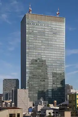
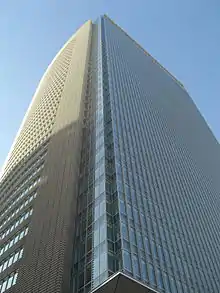
Tokyo Electron Limited (Japanese: 東京エレクトロン株式会社, Hepburn: Tokyo Erekutoron Kabushiki-gaisha), or TEL, is a Japanese electronics and semiconductor company headquartered in Akasaka, Minato-ku, Tokyo, Japan.[4] The company was founded as Tokyo Electron Laboratories, Inc. in 1963.
 | |
Native name | 東京エレクトロン株式会社 |
|---|---|
Romanized name | Tōkyō Erekutoron kabushiki gaisha |
| Formerly | Tokyo Electron Laboratories, Inc. (1963–1978) |
| Type | Public KK |
| |
| Industry | Electronics Semiconductors |
| Predecessor | Sakura Yoko KK founded on April 6, 1951 |
| Founded | November 11, 1963 (as Tokyo Electron Laboratories, Inc.) |
| Founder |
|
| Headquarters | , Japan |
Area served | Japan Taiwan North America South Korea Europe Southeast Asia China |
Key people | Tetsuro Higashi (CEO, President and Chairman) |
| Products |
|
| Revenue | |
| Total assets | |
| Total equity | |
Number of employees | 12,742 (2020)[2] |
| Parent | TBS Holdings, Inc. (4.67%) |
| Subsidiaries | 26 Group companies, including Tokyo Electron Device (TYO: 2760) |
| Website | tel.com |
| Footnotes / references [3][4][5][6] | |
TEL is best known as a supplier of equipment to fabricate integrated circuits (IC), flat panel displays (FPD), and photovoltaic cells (PV).[4] Tokyo Electron Device (東京エレクトロンデバイス株式会社, Tokyo Erekutoron Debaisu Kabushiki-gaisha, TYO: 2760), or TED, is a subsidiary of TEL specializing in semiconductor devices, electronic components, and networking devices.[4] As of 2011, TEL is the largest manufacturer of IC and FPD production equipment.[4]
On September 24, 2013 Tokyo Electron and Applied Materials announced a merger,[7] forming a new company to be called Eteris.[8][9] Eteris would have been the world's largest supplier of semiconductor processing equipment, with a total market value of approximately $29 billion. On 26 April 2015, the merger was cancelled due to antitrust concerns in the United States.[10]
Origins
On November 11, 1963, Tokyo Electron Laboratories Incorporated was founded by Tokuo Kubo and Toshio Kodaka, largely funded by Tokyo Broadcasting System (TBS), with a capital of over five million yen. Later that year, their office opened in the TBS main building and began manufacturing thousands of quality-control and importing diffusion furnaces made by Thermco and selling Japanese-made car radios.[11]
In 1965, the company approached a rapidly growing business in the market, Fairchild Semiconductor Corporation and agreed to serve as a sales agency for them, increasing their capital to twenty million yen and began exporting IC testers, IC sockets, IC connectors, and other similar computer components.[11]
The company opened an office in San Francisco, California and their new branch, Pan Electron in 1968 established themselves as the only stocking distributor of imported electronic components in the region.[11]
One year later, they opened their Yokohama office and established Teltron, a major manufacturer and distributor of car stereos, expanding their headquarters to fill the entire TBS-2 building and raising their capital to 100 million yen.[11]
Products
Semiconductor Production Equipment (SPE)
TEL produces Semiconductor Production Equipment (SPE) for the following purposes:[4]
- Thermal processing
- Deposition of thin layers of dielectric material between transistors onto the silicon wafer surface in a heated low-pressure chemical vapor deposition (LPCVD) or oxidation process[12]
- Photoresist coating/developing
- Photoresist coating and developing to project a microscopic circuitry pattern on the wafer in photolithography[13]
- Plasma etching[14]
- Wet surface preparation
- Wafer surface cleaning to remove foreign particles or contaminants such as dust[15]
- Single wafer chemical vapor deposition
- Deposition of thin layers of various materials, such as tungsten, tungsten silicide, titanium, titanium nitride, and tantalum oxide[16]
- Wafer probing
- Wafer probers for testing the functionality and performance of each die on the wafer[17]
- Material modification/doping
- Surface modification and doping using gas cluster ion beam (GCIB) technology[18]
- Corrective etching/trimming
- Corrective etching and trimming of thin films such as silicon, silicon nitride, silicon dioxide, aluminum nitride, and metals[19]
- Integrated metrology (co-developed by TEL and KLA Tencor)[20]
- Advanced Packaging[21]
Group companies
The Tokyo Electron Group consists of TEL and the following subsidiaries:[3][22]
- TEL Epion Inc.
- TEL FSI, Inc.
- TEL Solar
- TEL Technology Center, America, LLC
- TEL Venture Capital, Inc.
- Tokyo Electron Device Limited
- Tokyo Electron Yamanashi Limited
- Tokyo Electron Tohoku Limited
- Tokyo Electron Kyushu Limited
- Tokyo Electron Miyagi Limited
- Tokyo Electron Technology Development Institute, Inc.
- Tokyo Electron Software Technologies Limited
- Tokyo Electron FE Limited
- Tokyo Electron BP Limited
- Tokyo Electron PV Limited
- Tokyo Electron TS Limited
- Tokyo Electron Agency Limited
- Tokyo Electron U.S. Holdings, Inc.
- Tokyo Electron America, Inc.
- Tokyo Electron Europe Limited — Head Office (Crawley, England)
- German Branch
- Italian Branch
- Netherlands Branch
- Irish Branch
- French Branch
- Tokyo Electron Israel Limited
- Tokyo Electron Korea Limited
- Tokyo Electron Korea Solution Limited
- Tokyo Electron Taiwan Limited
- Tokyo Electron (Shanghai) Limited
- Tokyo Electron (Shanghai) Logistic Center Limited
- Tokyo Electron (Kunshan) Limited
- Timbre Technologies, Inc.
Research and development
TEL's Leading-edge Process Development Center is located in Nirasaki, Yamanashi. TEL also has the Kansai Technology Center in Amagasaki, Hyogo Prefecture and the Sendai Design and Development Center in Sendai, Miyagi Prefecture. TEL Technology Center, America, LLC in Albany, New York is the R&D center in the United States. TEL is one of the partners of IMEC, a microelectronics and nanoelectronics research center in Leuven, Belgium.[3]
In July 2014, TEL announced the establishment of joint assembly lab with Institute of Microelectronics in Singapore. The lab is focused on the research and development of Wafer Level Packaging and assembly, to address the need of Internet of Things with devices of high performance and low power consumption.[23]
Sponsorships
TEL supports association football in Japan by sponsoring the J. League as a whole and the football club Ventforet Kofu based in Kofu and Nirasaki as well as the rest of Yamanashi Prefecture.
The company has acquired naming rights of two multipurpose halls:
- "Tokyo Electron Nirasaki Ars Hall" (ja:韮崎市文化ホール) owned by Nirasaki City
- "Tokyo Electron Hall Miyagi" (ja:宮城県民会館) owned by Miyagi Prefecture (currently closed due to the heavy earthquake damage)
See also
References
- https://www.forbes.com/companies/tokyo-electron/#620acb5238c9
- https://www.forbes.com/companies/tokyo-electron/#620acb5238c9
- "Annual Report 2011" (PDF). Tokyo Electron Limited. March 31, 2011. Archived from the original (PDF) on January 4, 2012. Retrieved February 23, 2012.
- "Fact Book 2011" (PDF). Tokyo Electron Limited. March 31, 2011. Retrieved February 23, 2012.
- "Company Info". Tokyo Electron Limited. April 1, 2013. Retrieved March 11, 2014.
- "Tokyo Electron Ltd: TYO:8035 quotes & news - Google Finance". www.google.com.
- Pfanner, Michael J. de la Merced and Eric. "U.S. Manufacturer of Chip-Making Equipment Buys Japanese Rival".
- "WSJ" – via online.wsj.com.
- Editorial, Reuters. "${Instrument_CompanyName} ${Instrument_Ric} Key Developments - Reuters.com". U.S.
- "UPDATE 3-Applied Materials scraps Tokyo Electron takeover on U.S. antitrust concerns". 27 April 2015 – via Reuters.
- "Explore Our History". Tokyo Electron Limited. Archived from the original on March 1, 2012. Retrieved February 23, 2012.
- "Thermal Processing". Tokyo Electron Limited. Retrieved February 23, 2012.
- "Coater/Developers". Tokyo Electron Limited. Retrieved February 23, 2012.
- "Etch Systems". Tokyo Electron Limited. Retrieved February 23, 2012.
- "Surface Preparation Systems". Tokyo Electron Limited. Retrieved February 23, 2012.
- "Single Wafer Deposition". Tokyo Electron Limited. Retrieved February 23, 2012.
- "Wafer Probe Systems". Tokyo Electron Limited. Retrieved February 23, 2012.
- "Material Modification/Doping". Tokyo Electron Limited. Retrieved February 23, 2012.
- "Corrective Etching/Trimming". Tokyo Electron Limited. Retrieved February 23, 2012.
- "Integrated Metrology Systems". Tokyo Electron Limited. Retrieved February 23, 2012.
- "Advanced Packaging | Semiconductor Production Equipment | Tokyo Electron". www.tel.com. Retrieved 2016-03-16.
- "Locations | About TEL | Tokyo Electron". www.tel.com. Retrieved 2016-03-16.
- "Establishment of Joint Assembly Lab with Institute of Microelectronics in Singapore". Tokyo Electron Limited. Retrieved 29 July 2014.