800 nm process
The 800 nm process refers to the level of MOSFET semiconductor fabrication process technology that was reached around the 1987–1990 timeframe, by leading semiconductor companies like NTT, NEC, Toshiba, IBM, Hitachi, Matsushita, Mitsubishi Electric and Intel.
| Semiconductor device fabrication |
|---|
 |
|
(process nodes) |
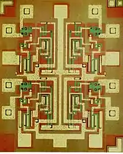
Products featuring 0.8 μm manufacturing process
- NTT introduced the 800 nm CMOS process for its 1 Mbit DRAM memory chip in 1984.[1]
- IBM's Bijan Davari developed high-performance, low-voltage, deep sub-micron CMOS technology in the mid-1980s, which enabled the development of faster computers as well as portable computers and battery-powered handheld electronics.[2]
- NEC and Toshiba used this process for their 4 Mbit DRAM memory chips in 1986.[3]
- Hitachi, IBM, Matsushita and Mitsubishi Electric used this process for their 4 Mbit DRAM memory chips in 1987.[1]
- Toshiba used the process for their 4 Mbit EPROM memory chip in 1987.[3]
- Hitachi, Mitsubishi and Toshiba used this process for their 1 Mbit SRAM memory chips in 1987.[3]
- Intel 80486 CPU, launched in 1989, was manufactured using this process.
- Intel i960CA CPU, announced in 1989, used this process.[4]
- microSPARC I launched in 1992.
- First Intel P5 Pentium CPUs at 60 MHz and 66 MHz launched in 1993. (BiCMOS)
References
- Gealow, Jeffrey Carl (10 August 1990). "Impact of Processing Technology on DRAM Sense Amplifier Design" (PDF). CORE. Massachusetts Institute of Technology. pp. 149–166. Retrieved 25 June 2019.
- "IEEE Andrew S. Grove Award Recipients". IEEE Andrew S. Grove Award. Institute of Electrical and Electronics Engineers. Retrieved 4 July 2019.
- "Memory". STOL (Semiconductor Technology Online). Retrieved 25 June 2019.
- "Intel i960 Embedded Microprocessor". National High Magnetic Field Laboratory. Florida State University. 3 March 2003. Archived from the original on 3 March 2003. Retrieved 29 June 2019.
| Preceded by 1 μm |
CMOS manufacturing processes | Succeeded by 600 nm |
This article is issued from Wikipedia. The text is licensed under Creative Commons - Attribution - Sharealike. Additional terms may apply for the media files.