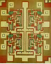
250 nm process
The 250 nm process refers to a level of MOSFET (CMOS) semiconductor process technology that was commercialized by semiconductor manufacturers around the 1996–1998 timeframe.
| Semiconductor device fabrication |
|---|
 |
|
(process nodes) |
A 250 nm CMOS process was demonstrated by a Japanese NEC research team led by Naoki Kasai in 1987.[1] In 1988, an IBM research team led by Iranian engineer Bijan Davari fabricated a 250 nm dual-gate MOSFET using a CMOS process.[2]
Products featuring 250 nm manufacturing process
- Hitachi introduced a 16 MB SRAM memory chip manufactured with this process in 1993.[3]
- Hitachi and NEC introduced 256 MB DRAM memory chips manufactured with this process in 1993, followed by Matsushita, Mitsubishi Electric and Oki in 1994.[3]
- NEC introduced a 1 Gb DRAM memory chip manufactured with this process in 1995.[3]
- Hitachi introduced a 128 MB NAND flash memory chip manufactured with this process in 1996.[3]
- The mobile Pentium MMX Tillamook, released in August 1997.
- The AMD K6-2 Chomper and Chomper Extended. Chomper was released on May 28, 1998.
- The AMD K6-III "Sharptooth" used 250 nm.
- The Intel Pentium II Deschutes, released in 1998.
- The Dreamcast console's Hitachi SH-4 CPU and PowerVR2 GPU, released in 1998.
- The Intel Pentium III Katmai, released in 1999.
- The DEC Alpha 21264A, which was made commercially available in 1999.
- The initial version of the Emotion Engine processor used in the PlayStation 2 console.
| Preceded by 350 nm |
CMOS manufacturing processes | Succeeded by 180 nm |
References
- Kasai, Naoki; Endo, Nobuhiro; Kitajima, Hiroshi (December 1987). "0.25 μm CMOS technology using P+polysilicon gate PMOSFET". 1987 International Electron Devices Meeting: 367–370. doi:10.1109/IEDM.1987.191433. S2CID 9203005.
- Davari, Bijan; et al. (1988). "A high-performance 0.25 micrometer CMOS technology". International Electron Devices Meeting. doi:10.1109/IEDM.1988.32749. S2CID 114078857.
- "Memory". STOL (Semiconductor Technology Online). Retrieved 25 June 2019.
This article is issued from Wikipedia. The text is licensed under Creative Commons - Attribution - Sharealike. Additional terms may apply for the media files.