AMD PowerTune
AMD PowerTune is a series of dynamic frequency scaling technologies built into some AMD GPUs and APUs that allow the clock speed of the processor to be dynamically changed (to different P-states) by software. This allows the processor to meet the instantaneous performance needs of the operation being performed, while minimizing power draw, heat generation and noise avoidance. AMD PowerTune aims to solve thermal design power and performance constraints.[1]
| Design firm | Advanced Micro Devices |
|---|---|
| Introduced | December 2011 |
| Type | Dynamic frequency scaling |
Besides the reduced energy consumption, AMD PowerTune helps to lower the noise levels created by the cooling in desktop computers, and extends battery life in mobile devices. AMD PowerTune is the successor to AMD PowerPlay.[2]
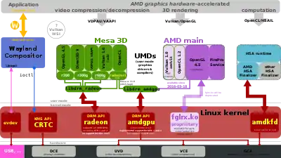
Support for "PowerPlay" was added to the Linux kernel driver "amdgpu" on November 11, 2015.[3]
As a lecture from CCC in 2014 shows, AMD's x86-64 SMU firmware is executed on some LatticeMico32 and PowerTune was modeled using Matlab.[4] This is similar to Nvidia's PDAEMON, the RTOS responsible for power on their GPUs.[5]
Overview

AMD PowerTune was introduced in the TeraScale 3 (VLIW4) with Radeon HD 6900 on 15 December 2010 and has been available in different development stages on Radeon- and AMD FirePro-branded products ever since.
Over the years, reviews which document the development of AMD PowerTune have been published by AnandTech.[6][7][8][9]
An additional technology named AMD ZeroCore Power has been available since the Radeon HD 7000 Series, implementing the Graphics Core Next microarchitecture.
The pointlessness of a fixed clock frequency was accredited in January 2014 by SemiAccurate.[10]
Operating system support
AMD Catalyst is available for Microsoft Windows and Linux and supports AMD PowerTune since version.
The free and open-source "Radeon" graphics device driver has some support for AMD PowerTune, see "Enduro".[11]
Feature overview for AMD APUs
The following table shows features of AMD's APUs (see also: List of AMD accelerated processing units).
| Codename | Server | Basic | Toronto | |||||||||||||||||
|---|---|---|---|---|---|---|---|---|---|---|---|---|---|---|---|---|---|---|---|---|
| Micro | Kyoto | |||||||||||||||||||
| Desktop | Performance | Renoir | ||||||||||||||||||
| Mainstream | Llano | Trinity | Richland | Kaveri | Kaveri Refresh (Godavari) | Carrizo | Bristol Ridge | Raven Ridge | Picasso | |||||||||||
| Entry | ||||||||||||||||||||
| Basic | Kabini | |||||||||||||||||||
| Mobile | Performance | Renoir | Cezanne | |||||||||||||||||
| Mainstream | Llano | Trinity | Richland | Kaveri | Carrizo | Bristol Ridge | Raven Ridge | Picasso | ||||||||||||
| Entry | Dalí | |||||||||||||||||||
| Basic | Desna, Ontario, Zacate | Kabini, Temash | Beema, Mullins | Carrizo-L | Stoney Ridge | |||||||||||||||
| Embedded | Trinity | Bald Eagle | Merlin Falcon, Brown Falcon |
Great Horned Owl | Grey Hawk | Ontario, Zacate | Kabini | Steppe Eagle, Crowned Eagle, LX-Family |
Prairie Falcon | Banded Kestrel | ||||||||||
| Platform | High, standard and low power | Low and ultra-low power | ||||||||||||||||||
| Released | Aug 2011 | Oct 2012 | Jun 2013 | Jan 2014 | 2015 | Jun 2015 | Jun 2016 | Oct 2017 | Jan 2019 | Mar 2020 | Jan 2021 | Jan 2011 | May 2013 | Apr 2014 | May 2015 | Feb 2016 | Apr 2019 | |||
| CPU microarchitecture | K10 | Piledriver | Steamroller | Excavator | "Excavator+"[12] | Zen | Zen+ | Zen 2 | Zen 3 | Bobcat | Jaguar | Puma | Puma+[13] | "Excavator+" | Zen | |||||
| ISA | x86-64 | x86-64 | ||||||||||||||||||
| Socket | Desktop | High-end | N/A | |||||||||||||||||
| Mainstream | N/A | FM2+[lower-alpha 1] | AM4 | |||||||||||||||||
| Entry | FM1 | FM2 | FM2+[lower-alpha 2] | AM1 | ||||||||||||||||
| Basic | N/A | N/A | ||||||||||||||||||
| Other | FS1 | FS1+, FP2 | FP3 | FP4 | FP5 | FP6 | FT1 | FT3 | FT3b | FP4 | FP5 | |||||||||
| PCI Express version | 2.0 | 3.0 | 4.0 | 2.0 | 3.0 | |||||||||||||||
| Fab. (nm) | GF 32SHP (HKMG SOI) |
GF 28SHP (HKMG bulk) |
GF 14LPP (FinFET bulk) |
GF 12LP (FinFET bulk) |
TSMC N7 (FinFET bulk) |
TSMC N40 (bulk) |
TSMC N28 (HKMG bulk) |
GF 28SHP (HKMG bulk) |
GF 14LPP (FinFET bulk) | |||||||||||
| Die area (mm2) | 228 | 246 | 245 | 245 | 250 | 210[14] | 156 | ? | 75 (+ 28 FCH) | 107 | ? | 125 | 149 | |||||||
| Min TDP (W) | 35 | 17 | 12 | 10 | 4.5 | 4 | 3.95 | 10 | 6 | |||||||||||
| Max APU TDP (W) | 100 | 95 | 65 | 18 | 25 | |||||||||||||||
| Max stock APU base clock (GHz) | 3 | 3.8 | 4.1 | 4.1 | 3.7 | 3.8 | 3.6 | 3.7 | 3.8 | ? | 1.75 | 2.2 | 2 | 2.2 | 3.2 | 3.3 | ||||
| Max APUs per node[lower-alpha 3] | 1 | 1 | ||||||||||||||||||
| Max CPU[lower-alpha 4] cores per APU | 4 | 8 | 2 | 4 | 2 | |||||||||||||||
| Max threads per CPU core | 1 | 2 | 1 | 2 | ||||||||||||||||
| Integer structure | 3+3 | 2+2 | 4+2 | 4+2+1 | ? | 1+1+1+1 | 2+2 | 4+2 | ||||||||||||
| i386, i486, i586, CMOV, NOPL, i686, PAE, NX bit, CMPXCHG16B, AMD-V, RVI, ABM, and 64-bit LAHF/SAHF | ||||||||||||||||||||
| IOMMU[lower-alpha 5] | N/A | |||||||||||||||||||
| BMI1, AES-NI, CLMUL, and F16C | N/A | |||||||||||||||||||
| MOVBE | N/A | |||||||||||||||||||
| AVIC, BMI2 and RDRAND | N/A | |||||||||||||||||||
| ADX, SHA, RDSEED, SMAP, SMEP, XSAVEC, XSAVES, XRSTORS, CLFLUSHOPT, and CLZERO | N/A | N/A | ||||||||||||||||||
| WBNOINVD, CLWB, RDPID, RDPRU, and MCOMMIT | N/A | N/A | ||||||||||||||||||
| FPUs per core | 1 | 0.5 | 1 | 1 | 0.5 | 1 | ||||||||||||||
| Pipes per FPU | 2 | 2 | ||||||||||||||||||
| FPU pipe width | 128-bit | 256-bit | 80-bit | 128-bit | ||||||||||||||||
| CPU instruction set SIMD level | SSE4a[lower-alpha 6] | AVX | AVX2 | SSSE3 | AVX | AVX2 | ||||||||||||||
| 3DNow! | 3DNow!+ | N/A | N/A | |||||||||||||||||
| PREFETCH/PREFETCHW | ||||||||||||||||||||
| FMA4, LWP, TBM, and XOP | N/A | N/A | N/A | N/A | ||||||||||||||||
| FMA3 | ||||||||||||||||||||
| L1 data cache per core (KiB) | 64 | 16 | 32 | 32 | ||||||||||||||||
| L1 data cache associativity (ways) | 2 | 4 | 8 | 8 | ||||||||||||||||
| L1 instruction caches per core | 1 | 0.5 | 1 | 1 | 0.5 | 1 | ||||||||||||||
| Max APU total L1 instruction cache (KiB) | 256 | 128 | 192 | 256 | 512 | 64 | 128 | 96 | 128 | |||||||||||
| L1 instruction cache associativity (ways) | 2 | 3 | 4 | 8 | 2 | 3 | 4 | |||||||||||||
| L2 caches per core | 1 | 0.5 | 1 | 1 | 0.5 | 1 | ||||||||||||||
| Max APU total L2 cache (MiB) | 4 | 2 | 4 | 1 | 2 | 1 | ||||||||||||||
| L2 cache associativity (ways) | 16 | 8 | 16 | 8 | ||||||||||||||||
| APU total L3 cache (MiB) | N/A | 4 | 8 | N/A | 4 | |||||||||||||||
| APU L3 cache associativity (ways) | 16 | 16 | ||||||||||||||||||
| L3 cache scheme | Victim | N/A | Victim | Victim | ||||||||||||||||
| Max stock DRAM support | DDR3-1866 | DDR3-2133 | DDR3-2133, DDR4-2400 | DDR4-2400 | DDR4-2933 | DDR4-3200, LPDDR4-4266 | LPDDR4-4266 | DDR3L-1333 | DDR3L-1600 | DDR3L-1866 | DDR3-1866, DDR4-2400 | DDR4-2400 | ||||||||
| Max DRAM channels per APU | 2 | 1 | 2 | |||||||||||||||||
| Max stock DRAM bandwidth (GB/s) per APU | 29.866 | 34.132 | 38.400 | 46.932 | 68.256 | ? | 10.666 | 12.800 | 14.933 | 19.200 | 38.400 | |||||||||
| GPU microarchitecture | TeraScale 2 (VLIW5) | TeraScale 3 (VLIW4) | GCN 2nd gen | GCN 3rd gen | GCN 5th gen[15] | TeraScale 2 (VLIW5) | GCN 2nd gen | GCN 3rd gen[15] | GCN 5th gen | |||||||||||
| GPU instruction set | TeraScale instruction set | GCN instruction set | TeraScale instruction set | GCN instruction set | ||||||||||||||||
| Max stock GPU base clock (MHz) | 600 | 800 | 844 | 866 | 1108 | 1250 | 1400 | 2100 | ? | 538 | 600 | ? | 847 | 900 | 1200 | |||||
| Max stock GPU base GFLOPS[lower-alpha 7] | 480 | 614.4 | 648.1 | 886.7 | 1134.5 | 1760 | 1971.2 | 2150.4 | ? | 86 | ? | ? | ? | 345.6 | 460.8 | |||||
| 3D engine[lower-alpha 8] | Up to 400:20:8 | Up to 384:24:6 | Up to 512:32:8 | Up to 704:44:16[16] | Up to 512:32:8 | ? | 80:8:4 | 128:8:4 | Up to 192:?:? | Up to 192:?:? | ||||||||||
| IOMMUv1 | IOMMUv2 | IOMMUv1 | ? | IOMMUv2 | ||||||||||||||||
| Video decoder | UVD 3.0 | UVD 4.2 | UVD 6.0 | VCN 1.0[17] | VCN 2.0[18] | UVD 3.0 | UVD 4.0 | UVD 4.2 | UVD 6.0 | UVD 6.3 | VCN 1.0 | |||||||||
| Video encoder | N/A | VCE 1.0 | VCE 2.0 | VCE 3.1 | N/A | VCE 2.0 | VCE 3.1 | |||||||||||||
| AMD Fluid Motion | ||||||||||||||||||||
| GPU power saving | PowerPlay | PowerTune | PowerPlay | PowerTune[19] | ||||||||||||||||
| TrueAudio | N/A | N/A | ||||||||||||||||||
| FreeSync | 1 2 |
1 2 | ||||||||||||||||||
| HDCP[lower-alpha 9] | ? | 1.4 | 1.4 2.2 | ? | 1.4 | 1.4 2.2 | ||||||||||||||
| PlayReady[lower-alpha 9] | N/A | 3.0 not yet | N/A | 3.0 not yet | ||||||||||||||||
| Supported displays[lower-alpha 10] | 2–3 | 2–4 | 3 | 3 (desktop) 4 (mobile, embedded) | 4 | 2 | 3 | 4 | ||||||||||||
/drm/radeon[lower-alpha 11][22][11] | N/A | N/A | ||||||||||||||||||
/drm/amdgpu[lower-alpha 11][23] | N/A | N/A | ||||||||||||||||||
- For FM2+ Excavator models: A8-7680, A6-7480 & Athlon X4 845.
- For FM2+ Excavator models: A8-7680, A6-7480 & Athlon X4 845.
- A PC would be one node.
- An APU combines a CPU and a GPU. Both have cores.
- Requires firmware support.
- No SSE4. No SSSE3.
- Single-precision performance is calculated from the base (or boost) core clock speed based on a FMA operation.
- Unified shaders : texture mapping units : render output units
- To play protected video content, it also requires card, operating system, driver, and application support. A compatible HDCP display is also needed for this. HDCP is mandatory for the output of certain audio formats, placing additional constraints on the multimedia setup.
- To feed more than two displays, the additional panels must have native DisplayPort support.[21] Alternatively active DisplayPort-to-DVI/HDMI/VGA adapters can be employed.
- DRM (Direct Rendering Manager) is a component of the Linux kernel. Support in this table refers to the most current version.
Feature overview for AMD graphics cards
The following table shows features of AMD's GPUs (see also: List of AMD graphics processing units).
| Name of GPU series | Wonder | Mach | 3D Rage | Rage Pro | Rage | R100 | R200 | R300 | R400 | R500 | R600 | RV670 | R700 | Evergreen | Northern Islands |
Southern Islands |
Sea Islands |
Volcanic Islands |
Arctic Islands/Polaris |
Vega | Navi | Big Navi | |||
|---|---|---|---|---|---|---|---|---|---|---|---|---|---|---|---|---|---|---|---|---|---|---|---|---|---|
| Released | 1986 | 1991 | 1996 | 1997 | 1998 | Apr 2000 | Aug 2001 | Sep 2002 | May 2004 | Oct 2005 | May 2007 | Nov 2007 | Jun 2008 | Sep 2009 | Oct 2010 | Jan 2012 | Sep 2013 | Jun 2015 | Jun 2016 | Jun 2017 | Jul 2019 | Nov 2020 | |||
| Marketing Name | Wonder | Mach | 3D Rage | Rage Pro | Rage | Radeon 7000 | Radeon 8000 | Radeon 9000 | Radeon X700/X800 | Radeon X1000 | Radeon HD 2000 | Radeon HD 3000 | Radeon HD 4000 | Radeon HD 5000 | Radeon HD 6000 | Radeon HD 7000 | Radeon Rx 200 | Radeon Rx 300 | Radeon RX 400/500 | Radeon RX Vega/Radeon VII(7nm) | Radeon RX 5000 | Radeon RX 6000 | |||
| AMD support | |||||||||||||||||||||||||
| Kind | 2D | 3D | |||||||||||||||||||||||
| Instruction set | Not publicly known | TeraScale instruction set | GCN instruction set | RDNA instruction set | |||||||||||||||||||||
| Microarchitecture | TeraScale 1 | TeraScale 2 (VLIW5) | TeraScale 3 (VLIW4) | GCN 1st gen | GCN 2nd gen | GCN 3rd gen | GCN 4th gen | GCN 5th gen | RDNA | RDNA 2 | |||||||||||||||
| Type | Fixed pipeline[lower-alpha 1] | Programmable pixel & vertex pipelines | Unified shader model | ||||||||||||||||||||||
| Direct3D | N/A | 5.0 | 6.0 | 7.0 | 8.1 | 9.0 11 (9_2) |
9.0b 11 (9_2) |
9.0c 11 (9_3) |
10.0 11 (10_0) |
10.1 11 (10_1) |
11 (11_0) | 11 (11_1) 12 (11_1) |
11 (12_0) 12 (12_0) |
11 (12_1) 12 (12_1) |
11 (12_2) 12 (12_2) | ||||||||||
| Shader model | N/A | 1.4 | 2.0+ | 2.0b | 3.0 | 4.0 | 4.1 | 5.0 | 5.1 | 5.1 6.3 |
6.4 | 6.5 | |||||||||||||
| OpenGL | N/A | 1.1 | 1.2 | 1.3 | 2.0[lower-alpha 2] | 3.3 | 4.5 (on Linux + Mesa 3D: 4.5 with FP64 HW support, 4.3 without)[25][26][27][lower-alpha 3] | 4.6 (on Linux: 4.6 (Mesa 20.0)) | |||||||||||||||||
| Vulkan | N/A | 1.0 (Win 7+ or Mesa 17+) |
1.2 (Adrenalin 20.1, Linux Mesa 20.0) | ||||||||||||||||||||||
| OpenCL | N/A | Close to Metal | 1.1 | 1.2 | 2.0 (Adrenalin driver on Win7+) (on Linux: 1.2 with Mesa 3D, 2.1 with AMD drivers or AMD ROCm) |
? | 2.1 [28] | ||||||||||||||||||
| HSA | N/A | ? | |||||||||||||||||||||||
| Video decoding ASIC | N/A | Avivo/UVD | UVD+ | UVD 2 | UVD 2.2 | UVD 3 | UVD 4 | UVD 4.2 | UVD 5.0 or 6.0 | UVD 6.3 | UVD 7[29][lower-alpha 4] | VCN 2.0[29][lower-alpha 4] | VCN 3.0[30] | ||||||||||||
| Video encoding ASIC | N/A | VCE 1.0 | VCE 2.0 | VCE 3.0 or 3.1 | VCE 3.4 | VCE 4.0[29][lower-alpha 4] | |||||||||||||||||||
| Fluid Motion | |||||||||||||||||||||||||
| Power saving | ? | PowerPlay | PowerTune | PowerTune & ZeroCore Power | ? | ||||||||||||||||||||
| TrueAudio | N/A | Via dedicated DSP | Via shaders | ? | |||||||||||||||||||||
| FreeSync | N/A | 1 2 | |||||||||||||||||||||||
| HDCP[lower-alpha 5] | ? | 1.4 | 1.4 2.2 |
1.4 2.2 2.3 |
? | ||||||||||||||||||||
| PlayReady[lower-alpha 5] | N/A | 3.0 | 3.0 | ? | |||||||||||||||||||||
| Supported displays[lower-alpha 6] | 1–2 | 2 | 2–6 | ? | |||||||||||||||||||||
| Max. resolution | ? | 2–6 × 2560×1600 |
2–6 × 4096×2160 @ 60 Hz |
2–6 × 5120×2880 @ 60 Hz |
3 × 7680×4320 @ 60 Hz[31] |
? | |||||||||||||||||||
/drm/radeon[lower-alpha 7] |
N/A | ||||||||||||||||||||||||
/drm/amdgpu[lower-alpha 7] |
N/A | Experimental[32] | |||||||||||||||||||||||
- The Radeon 100 Series has programmable pixel shaders, but do not fully comply with DirectX 8 or Pixel Shader 1.0. See article on R100's pixel shaders.
- These series do not fully comply with OpenGL 2+ as the hardware does not support all types of non-power of two (NPOT) textures.
- OpenGL 4+ compliance requires supporting FP64 shaders and these are emulated on some TeraScale chips using 32-bit hardware.
- The UVD and VCE were replaced by the Video Core Next (VCN) ASIC in the Raven Ridge APU implementation of Vega.
- To play protected video content, it also requires card, operating system, driver, and application support. A compatible HDCP display is also needed for this. HDCP is mandatory for the output of certain audio formats, placing additional constraints on the multimedia setup.
- More displays may be supported with native DisplayPort connections, or splitting the maximum resolution between multiple monitors with active converters.
- DRM (Direct Rendering Manager) is a component of the Linux kernel. Support in this table refers to the most current version.
See also
- AMD Cool'n'Quiet (for desktop CPUs)
- AMD PowerNow! (for laptop CPUs)
- AMD Turbo Core (for CPUs)
- AMD PowerXpress (for multi-GPUs)
- Dynamic frequency scaling
- Intel SpeedStep (for CPUs)
- Intel Turbo Boost (for CPUs)
References
- "AMD PowerTune Technology" (pdf). AMD. 23 March 2012.
- "AMD PowerTune vs PowerPlay" (PDF). AMD. 1 December 2010. Archived from the original (pdf) on 14 July 2014. Retrieved 13 July 2014.
- "Add amdgpu powerplay support". 11 November 2015.
- "AMD x86 SMU firmware analysis". 27 December 2014.
- "Reverse engineering power management on Nvidia GPUs" (PDF).
- "Redefining TDP With PowerTune". AnandTech. 15 December 2010.
- "Introducing PowerTune Technology With Boost". AnandTech. 22 June 2012.
- "The New PowerTune: Adding Further States". AnandTech. 22 March 2013.
- "PowerTune: Improved Flexibility & Fan Speed Throttling". AnandTech. 23 October 2014.
- "What is AMD's PowerTune 2.0 and what does it do?". SemiAccurate. 16 December 2013.
- "Radeon feature matrix". freedesktop.org. Retrieved 10 January 2016.
- "AMD Announces the 7th Generation APU: Excavator mk2 in Bristol Ridge and Stoney Ridge for Notebooks". 31 May 2016. Retrieved 3 January 2020.
- "AMD Mobile "Carrizo" Family of APUs Designed to Deliver Significant Leap in Performance, Energy Efficiency in 2015" (Press release). 20 November 2014. Retrieved 16 February 2015.
- "The Mobile CPU Comparison Guide Rev. 13.0 Page 5 : AMD Mobile CPU Full List". TechARP.com. Retrieved 13 December 2017.
- "AMD VEGA10 and VEGA11 GPUs spotted in OpenCL driver". VideoCardz.com. Retrieved 6 June 2017.
- Cutress, Ian (1 February 2018). "Zen Cores and Vega: Ryzen APUs for AM4 – AMD Tech Day at CES: 2018 Roadmap Revealed, with Ryzen APUs, Zen+ on 12nm, Vega on 7nm". Anandtech. Retrieved 7 February 2018.
- Larabel, Michael (17 November 2017). "Radeon VCN Encode Support Lands in Mesa 17.4 Git". Phoronix. Retrieved 20 November 2017.
- Liu, Leo (4 September 2020). "Add Renoir VCN decode support". Retrieved 11 September 2020.
It has same VCN2.x block as Navi1x
- Tony Chen; Jason Greaves, "AMD's Graphics Core Next (GCN) Architecture" (PDF), AMD, retrieved 13 August 2016
- "A technical look at AMD's Kaveri architecture". Semi Accurate. Retrieved 6 July 2014.
- "How do I connect three or More Monitors to an AMD Radeon™ HD 5000, HD 6000, and HD 7000 Series Graphics Card?". AMD. Retrieved 8 December 2014.
- Airlie, David (26 November 2009). "DisplayPort supported by KMS driver mainlined into Linux kernel 2.6.33". Retrieved 16 January 2016.
- Deucher, Alexander (16 September 2015). "XDC2015: AMDGPU" (PDF). Retrieved 16 January 2016.
- Michel Dänzer (17 November 2016). "[ANNOUNCE] xf86-video-amdgpu 1.2.0". lists.x.org.
- "AMD Radeon Software Crimson Edition Beta". AMD. Retrieved 20 April 2018.
- "Mesamatrix". mesamatrix.net. Retrieved 22 April 2018.
- "RadeonFeature". X.Org Foundation. Retrieved 20 April 2018.
- "AMD Radeon RX 6800 XT Specs". TechPowerUp. Retrieved 1 January 2021.
- Killian, Zak (22 March 2017). "AMD publishes patches for Vega support on Linux". Tech Report. Retrieved 23 March 2017.
- Larabel, Michael (15 September 2020). "AMD Radeon Navi 2 / VCN 3.0 Supports AV1 Video Decoding". Phoronix. Retrieved 1 January 2021.
- "Radeon's next-generation Vega architecture" (PDF). Radeon Technologies Group (AMD). Archived from the original (PDF) on 6 September 2018. Retrieved 13 June 2017.
- Larabel, Michael (7 December 2016). "The Best Features of the Linux 4.9 Kernel". Phoronix. Retrieved 7 December 2016.